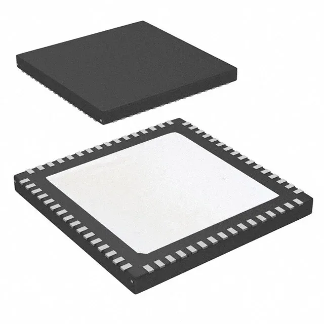
2.5 GHz jitter cleaner — what it buys the clock tree
The LMK04826BISQ/NOPB is a PLLatinum jitter cleaner from Texas Instruments, built to scrub phase noise from a reference clock and synthesize a clean output up to 2.5 GHz. That frequency ceiling covers the reference clocks for most high-speed ADCs, DACs, and FPGA transceivers up to 12 Gbps line rates. The part integrates a single PLL with a 3:15 input-to-output ratio, meaning you can feed it three reference sources and distribute fifteen cleaned clocks across the board.
Supply rail tolerance — why 3.3V needs to stay tight
The supply range is 3.15 V to 3.45 V — a narrow window that demands a regulated 3.3 V rail with less than 5 % total tolerance including ripple. If your board's 3.3 V bus droops to 3.0 V under load, this part is out of spec. Plan a low-noise LDO or a switching regulator with post-filter for this rail.
Signal interface flexibility — matching the I/O banks
Inputs accept LVCMOS, LVDS, or LVPECL levels, which covers the common oscillator and reference output formats. Outputs can be programmed as HSDS, LCPECL, LVCMOS, LVDS, or LVPECL — that's five format options, so the same part can feed a LVPECL ADC clock input on one bank and an LVDS FPGA reference on another. All I/O pairs are differential-capable, which is the right choice for routing clean clocks across a noisy digital board.
It belongs in outdoor telecom base stations, factory-floor Ethernet switches, and instrumentation that lives in an unheated enclosure. Not a commercial 0-70°C part — if your BOM calls for this code, the design already expects the extended range.