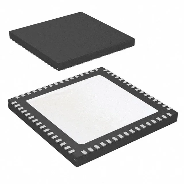
Dual PLL jitter cleaner for high-speed converter clock trees
The LMK04816BISQE/NOPB is a dual PLL jitter-cleaning clock IC from TI's PLLatinum™ family, designed to generate low-jitter clock sources for high-speed ADCs, DACs, and data converters. Its 2.6 GHz maximum output frequency covers the clock rates needed for 10+ GSPS converters and JESD204B interfaces. With a 3:12 input-to-output ratio, this chip accepts up to three reference inputs and produces twelve independent clock outputs — enough to clock an entire multi-board data-acquisition system from a single device. The differential input and output paths (Yes/Yes) maintain signal integrity over long board traces.
Flexible I/O and supply rail planning
Both the input and output stages accept LVCMOS, LVDS, and LVPECL levels, so the chip can interface directly with a crystal oscillator, a VCXO, or another PLL without external level translators. The 3.15 V to 3.45 V supply range is tight — the LDO feeding this rail should be a low-noise type with better than 1% regulation to keep the PLL's in-band phase noise low. The 64-WFQFN exposed pad (9x9 mm) is hand-solderable with a hot-air station, but the thermal pad must be stitched to a ground plane with a via array to meet the datasheet's thermal resistance.