2.6 GHz jitter cleaner — what the frequency ceiling buys you
The LMK04816BISQ/NOPB is a PLLatinum clock jitter cleaner from Texas Instruments that synthesises and cleans clocks up to 2.6 GHz. It accepts three reference inputs (LVCMOS, LVDS, or LVPECL) and distributes twelve clock outputs in the same logic families — enough to feed a multi-channel ADC array, an FPGA fabric, and a system reference from one device. The 2.6 GHz ceiling covers the sample-clock range for most GSPS ADCs and the reference clock for JESD204B SerDes lanes. If your ADC or FPGA requires a clock above 2.6 GHz, this part is not the fit; below that, it is the jitter-cleaning anchor of the clock tree.
Supply rail tolerance — a common BOM trap
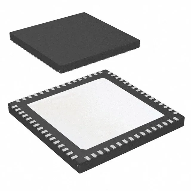
The supply range is 3.15 V to 3.45 V — a 300 mV window that demands a 3.3 V rail regulated to ±1 %. Budget a low-noise LDO with 1 % set-point accuracy on this rail. The 64-WQFN (9x9) exposed pad requires a thermal-via array under the centre pad to keep the die temperature within the lock-range window.
3:12 fan-out — one PLL replaces a distribution buffer
Three reference inputs and twelve outputs let this single PLL absorb the function of a clock generator plus a fan-out buffer. The differential inputs and outputs are all differential-capable (Yes/Yes), so the LVDS or LVPECL paths maintain signal integrity over backplane traces without external translation. The divider/multiplier is present (Yes) but the multiplier function is not enabled (No) — this is a fractional-N or integer-N PLL depending on the configuration, not a clock multiplier. For pure multiplication look at the LMK04828 family; this part is optimised for jitter cleaning and distribution.
The base product number is LMK04816, so the BISQ/NOPB suffix identifies the 64-WQFN package with lead-free (NOPB) finish.