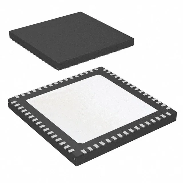
Jitter cleaner PLL for high-speed clock distribution
The Texas Instruments LMK04806BISQE/NOPB is a PLLatinum™ jitter cleaner PLL designed to reduce phase noise and jitter on reference clocks for high-speed data converters, RF transceivers, and FPGA-based systems. The 2:14 input-to-output ratio provides two reference inputs that can be fanned out to 14 differential or single-ended clock outputs, each individually configurable as LVCMOS, LVDS, or LVPECL. Operating from a 3.15 V to 3.45 V supply and rated over the -40°C to 85°C industrial temperature range, it suits outdoor telecom base stations, radar/signal-intelligence receivers, and instrumentation that must hold timing margin across environmental extremes.
1.536 GHz max frequency — what it buys the clock tree
The 1.536 GHz maximum output frequency covers the reference clock rates for most high-speed ADCs (e.g., JESD204B subclass 1 devices) and RF synthesizers. At these frequencies, the jitter cleaner loop bandwidth is typically set between 10 Hz and 100 kHz to attenuate close-in phase noise from the reference source. The dual-PLL architecture lets one PLL clean the reference while the other synthesizes the output, so the designer can trade off loop bandwidth versus lock time independently.
Supply and interface — 3.3 V only, no surprises
The supply range is 3.15 V to 3.45 V, which means this is a 3.3 V ±5% part. The input and output signal formats — LVCMOS, LVDS, LVPECL — are all 3.3 V compatible; if the downstream device uses a lower-voltage logic family (e.g., 1.8 V CML), a DC-blocking capacitor or level shifter is needed on the output.
Package and thermal — 64-WQFN with exposed pad
ROHS3 compliant. The base product number is LMK04806, so the same die is available in other package or tape options under that base.