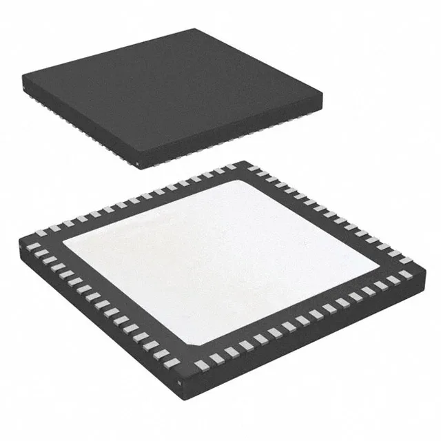
Active production — BOM-fit for timing trees
The LMK04805BISQE/NOPB: This is a single-PLL jitter cleaner (PLLatinum series) with a 2:14 input-to-output ratio, meaning it accepts two reference inputs and distributes up to fourteen cleaned clock outputs — enough to clock an entire ADC/DAC bank or a multi-SERDES backplane from one device. The maximum output frequency of 1.536 GHz covers the common ADC sampling clocks (up to 1.5 GSPS) and 10GbE SERDES reference clocks, but does not reach the 2+ GHz range needed for 25GbE or 56G PAM4 — check the VCO tuning range against your target frequency before committing the BOM line.
Supply rail and signal-level constraints
The supply voltage range is 3.15 V to 3.45 V — a tight 300 mV window around the nominal 3.3 V rail. The board's 3.3 V regulator must hold ±4.5% tolerance under load; a 3.3 V rail that droops to 3.1 V during a transient will pull the PLL out of lock. Input and output signal formats are LVCMOS, LVDS, and LVPECL — all differential-capable. The output type must match the downstream device's clock input standard; driving an LVDS input with an LVPECL output requires AC-coupling and termination resistors, adding two components per trace.
Temperature grade and deployment envelope
This covers base-station cabinets, outdoor small cells, and factory-floor instrumentation, but not under-hood automotive (125°C) or avionics (extended range). The part is surface-mount only (64-WQFN) and is supplied in tape-and-reel or cut-tape options — suitable for reflow assembly with a standard lead-free profile. The exposed pad demands a solder paste coverage of at least 50% under the pad for reliable thermal and electrical contact.