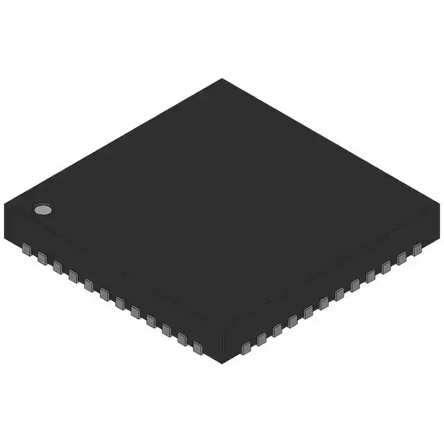
The LMK04110SQE/NOPB: The part ships in Tape & Reel (TR) packaging, 48-WFQFN Exposed Pad, surface-mount. Store the reels dry — the exposed-pad QFN is moisture-sensitive; a bake cycle before reflow is standard if the moisture-barrier bag is compromised.
1.08 GHz jitter cleaning — the clock-tree decision
The PLL core cleans jitter on reference clocks up to 1.08 GHz, accepting LVCMOS, LVDS, or LVPECL inputs and delivering 2VPECL or LVPECL outputs. Both the input and output paths are differential — this matters for signal integrity over longer board traces or when feeding high-speed ADCs and FPGAs that expect a differential reference. The 2:5 input-to-output ratio means two reference inputs feed five cleaned clock outputs. That is enough to distribute a low-jitter clock to multiple converters or logic devices from a single PLL, reducing the number of clock-tree stages and the associated phase-noise accumulation. Supply voltage is 3.15 V to 3.45 V — a tight window. The board's 3.3 V rail must stay within this band under load; a 3.3 V LDO with ±1% tolerance is a safe choice to keep the PLL in lock across temperature.
Industrial temperature grade — deployment context
The PLL's lock range and jitter performance are characterized across this band in the datasheet — expect the phase-noise floor to shift at the temperature extremes, but the device stays within spec.
Cross-reference check — LMK04111SQE/NOPB
For a pick-and-place line, the reel format is the standard — the bulk variant is more common for prototyping or small-run rework. The footprints are identical, so a board designed for one accepts the other without a layout change.