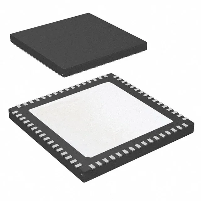
Texas Instruments LMK03806BISQ/NOPB — Clock & Timing ICs

Texas Instruments LMK03806BISQ/NOPB Clock IC, 2.6 GHz PLL

MPNLMK03806BISQ/NOPB
Active

Texas Instruments LMK03806BISQ/NOPB clock generator IC, PLL with bypass, 2.6 GHz max frequency, 1:14 fanout, LVCMOS/LVDS/LVPECL I/O, 64-WFQFN exposed pad, -40°C to 85°C.

$15.2800Ref. price · indicative, final on quote
Independent supplier — new & surplus stockAuthenticity-screened · ESD-safe packingListing updated Aug 2026

Specifications

LMK03806BISQ/NOPB specifications
ParameterValue
MountingSurface Mount
Supply voltage3.15V ~ 3.45V
Frequency - max2.6GHz
Operating temperature-40°C~85°C
PLLYes with Bypass
InputLVCMOS, LVDS, LVPECL, Crystal
OutputLVCMOS, LVDS, LVPECL
PackageTape & Reel (TR); Cut Tape (CT)
Case64-WFQFN Exposed Pad
Divider (Multiplier)Yes/No
Number of circuits1
Ratio - Input:Output1:14
Differential - Input:OutputYes/Yes

Product details

2.6 GHz PLL clock tree in a 1:14 fanout

The Texas Instruments LMK03806BISQ/NOPB is a clock generator with an integrated PLL that can be bypassed, delivering up to 2.6 GHz on its outputs. The 1:14 input-to-output ratio means a single reference clock fans out to fourteen independent clock domains, each programmable for frequency and format. Input accepts LVCMOS, LVDS, LVPECL, or a crystal oscillator; outputs are available in LVCMOS, LVDS, or LVPECL levels. This multi-protocol I/O eliminates external level translators when interfacing with FPGAs, SERDES, or ASICs that use different signalling standards.

Supply rail and package — what the board layout needs

The device operates from a 3.15 V to 3.45 V supply — a tight 300 mV window. The supply rail should be clean, with ripple below 10 mVpp, because PLL phase noise is directly sensitive to supply noise. A dedicated LDO per supply pin is common practice. The datasheet's recommended footprint includes a 5×5 via grid; skipping the vias raises the junction temperature by 15-20°C under full fanout load.

Temperature grade and deployment context

It fits outdoor radio units, base-station timing cards, and networking switches that sit in uncontrolled enclosures. The PLL maintains lock across the full range without external temperature compensation. This is a current-production part suitable for new designs and volume builds.

Frequently asked questions

What is the maximum output frequency of the LMK03806BISQ/NOPB?

The maximum output frequency is 2.6 GHz. This sets the upper limit for clocking high-speed SERDES interfaces or RF data converters directly from the PLL outputs.

Can the LMK03806BISQ/NOPB accept a crystal as its reference?

Yes, the input accepts a crystal oscillator in addition to LVCMOS, LVDS, and LVPECL references. This allows a low-cost fundamental-mode crystal to serve as the PLL reference without an external oscillator module.

How many clock outputs does the LMK03806BISQ/NOPB provide?

The part has a 1:14 input-to-output ratio, meaning it can generate up to fourteen independent clock outputs from a single reference. Each output can be independently programmed for frequency, format (LVCMOS, LVDS, LVPECL), and phase.