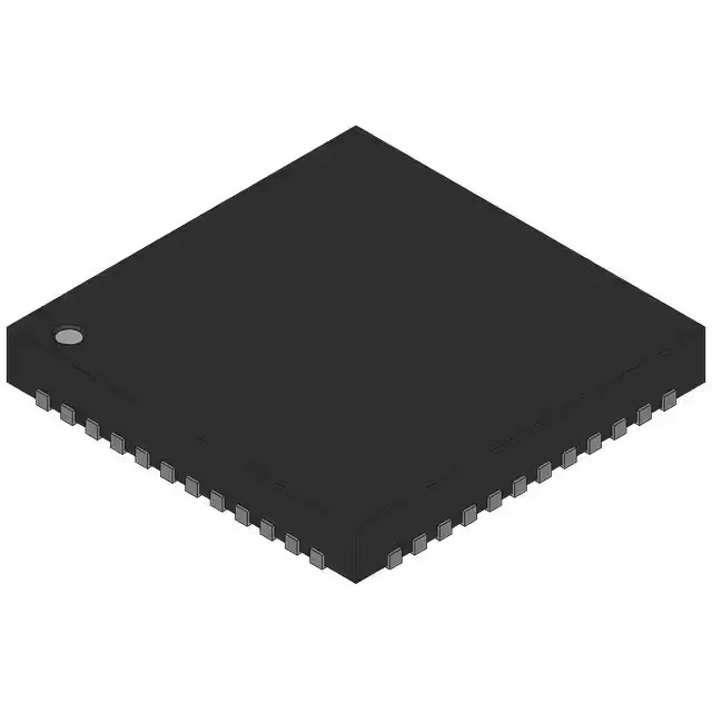
Texas Instruments LMK03001DISQ/NOPB — Clock & Timing ICs

LMK03001DISQ/NOPB Clock Conditioner, 1.57 GHz, 1:8 Fanout

MPNLMK03001DISQ/NOPB
Active

Texas Instruments LMK03001DISQ/NOPB precision clock conditioner, 1.57 GHz max, 1:8 LVDS/LVPECL fanout, 3.15-3.45V supply, -40 to 85°C, 48-WQFN exposed pad, Tape & Reel.

$17.5050Ref. price · indicative, final on quote
Packaging48-WFQFN Exposed Pad
Independent supplier — new & surplus stockAuthenticity-screened · ESD-safe packingListing updated Aug 2026

Specifications

LMK03001DISQ/NOPB specifications
ParameterValue
TypeClock Conditioner
MountingSurface Mount
Voltage3.15V ~ 3.45V
Frequency1.57GHz
Operating temperature-40°C~85°C
PLLNo
InputLVCMOS, LVDS, LVPECL
OutputLVDS, LVPECL
PackageTape & Reel (TR)
Case48-WFQFN Exposed Pad
Divider (Multiplier)Yes/No
Number of circuits1
Ratio - Input:Output1:8
Differential - Input:OutputYes/Yes

Product details

1.57 GHz clock conditioner with 1:8 LVDS/LVPECL fanout

It accepts LVCMOS, LVDS, or LVPECL inputs and provides eight LVDS or LVPECL outputs with a 1:8 fanout ratio, operating at frequencies up to 1.57 GHz. Unlike a PLL-based synthesizer, this part focuses on cleaning and redistributing an existing clock — it includes a divider but no multiplier. The 3.15 V to 3.45 V supply range demands a clean 3.3 V rail, and the industrial temperature rating (-40°C to 85°C) suits telecom infrastructure, base stations, data converters, and FPGA reference clock trees.

The 1.57 GHz maximum frequency covers the highest-speed serial interfaces — 10G Ethernet, CPRI, JESD204B converter clocks, and FPGA transceiver reference clocks. If your design runs below 1 GHz, the part still provides margin for the distribution path. The differential input and output paths (LVDS, LVPECL) keep signal integrity intact across the eight fanout channels, which matters when driving multiple ADC/DAC or SerDes devices from a single clean source.

Package and layout: 48-WQFN with exposed pad

Housed in a 48-WQFN (7x7 mm) with an exposed thermal pad, this part needs a solid via-stitched ground plane under the pad for both thermal relief and a low-inductance return path. The supply is a tight 3.15 V to 3.45 V — a 3.3 V rail with ±4.5% regulation. Decoupling at the supply pins with 0.1 µF and 1 µF ceramics close to the package is standard practice for this frequency range.

That means no last-time-buy urgency and no forced redesign for new builds. The -DISQ/NOPB suffix indicates the Tape & Reel variant with lead-free (NOPB) finish, which is the standard production ordering option.

Frequently asked questions

What is the maximum output frequency of LMK03001DISQ/NOPB?

The maximum frequency is 1.57 GHz. This covers the highest-speed serial interface clocks — 10G Ethernet, CPRI, JESD204B, and FPGA transceiver reference clocks — with margin for distribution losses.

Does LMK03001DISQ/NOPB support LVDS output?

Yes, the outputs can be configured as LVDS or LVPECL. The inputs accept LVCMOS, LVDS, or LVPECL, and all I/O paths are differential-capable.

Can LMK03001DISQ/NOPB be used as a replacement for LMK03001CISQ?

Both parts share the base product number LMK03001 and the same functional block — 1:8 clock conditioner with 1.57 GHz max frequency. The suffix differences (-DISQ vs -CISQ) typically indicate packaging or temperature grade variants. Verify the specific suffix requirements against your BOM before substituting; the -DISQ/NOPB is the lead-free Tape & Reel version.