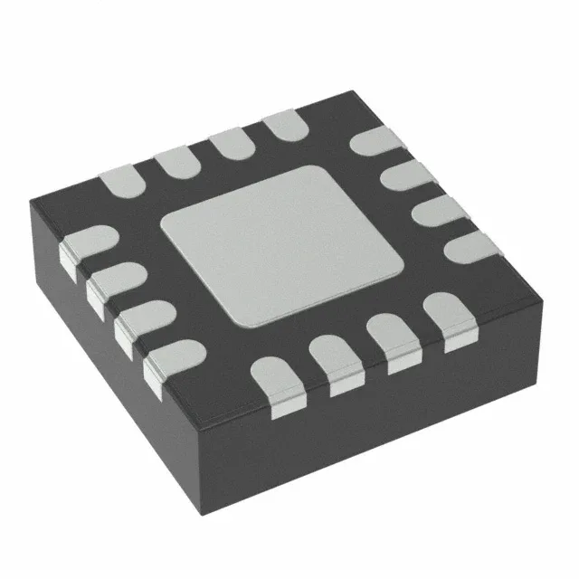
Texas Instruments LMK00804BQWRGTTQ1 — Clock & Timing ICs

TI LMK00804BQWRGTTQ1 Fanout Buffer, 350 MHz, AEC-Q100

MPNLMK00804BQWRGTTQ1
Active

Texas Instruments LMK00804BQWRGTTQ1, Automotive AEC-Q100 Fanout Buffer (Distribution), 2:4 ratio, 350 MHz max, 1.425V–3.465V supply, 16-VFQFN Exposed Pad, -40°C to 125°C.

$8.6300Ref. price · indicative, final on quote
Independent supplier — new & surplus stockAuthenticity-screened · ESD-safe packingListing updated Aug 2026

Specifications

LMK00804BQWRGTTQ1 specifications
ParameterValue
TypeFanout Buffer (Distribution)
SeriesAutomotive, AEC-Q100
MountingSurface Mount, Wettable Flank
Supply voltage1.425V ~ 3.465V
Frequency - max350 MHz
Operating temperature-40°C~125°C(TA)
InputHCSL, LVCMOS, LVDS, LVHSTL, LVPECL, LVTTL, SSTL
OutputLVCMOS, LVTTL
PackageTape & Reel (TR); Cut Tape (CT)
Case16-VFQFN Exposed Pad
Number of circuits1
Ratio - Input:Output2:4
Differential - Input:OutputYes/No

Product details

350 MHz fanout buffer for automotive clock trees

The LMK00804BQWRGTTQ1 is a 2:4 fanout buffer — two input channels each distribute to two outputs, giving four LVCMOS/LVTTL outputs from differential or single-ended sources. The 350 MHz maximum frequency sets the ceiling for clock distribution; at that rate the output rise time into the load capacitance, not the buffer itself, limits the usable fan-out in a real PCB trace. Input compatibility spans HCSL, LVCMOS, LVDS, LVHSTL, LVPECL, LVTTL, and SSTL — this covers the common clock sources from PCIe reference oscillators to FPGA differential outputs.

AEC-Q100 Grade 1 — the temperature band for under-hood and engine bay

The 125°C upper limit aligns with under-hood and engine-bay environments where a 105°C summer soak still leaves margin.

Package footprint and thermal pad design rule

Housed in a 16-VFQFN with exposed pad, 3x3 mm body (supplier device package 16-VQFN). The wettable flank option aids AOI inspection after reflow — the side solder fillet is visible to the camera, which standard QFN side-wall plating does not guarantee. The exposed pad must be soldered to the PCB ground plane to achieve the datasheet thermal resistance; a 3x3 mm pad with at least nine thermal vias under the die attach area is the typical layout rule.

Frequently asked questions

What input signal types does LMK00804BQWRGTTQ1 accept?

The buffer accepts HCSL, LVCMOS, LVDS, LVHSTL, LVPECL, LVTTL, and SSTL inputs. The differential inputs (HCSL, LVDS, LVHSTL, LVPECL, SSTL) are accepted on one pair of input pins, while the single-ended LVCMOS/LVTTL inputs are on the other pair — the 2:4 ratio means each input fans to two outputs.