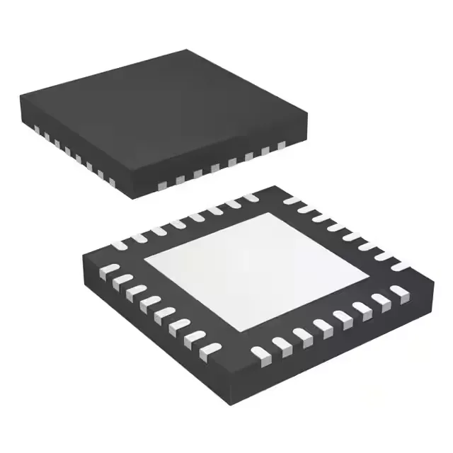
3:5 differential fanout buffer, no PLL
The LMK00334RTVT is a 3:5 differential fanout buffer from Texas Instruments, designed to distribute reference clocks for PCI Express and SATA CPU interfaces. It accepts a wide range of input standards — CML, HCSL, HSTL, LVDS, LVPECL, SSTL, and crystal — and outputs HCSL or LVCMOS levels. Because it has no internal PLL (PLL: No), this device does not perform jitter cleaning or frequency synthesis. It simply buffers and fans out an incoming clock to multiple destinations, preserving the input's phase noise profile. If your application needs to clean up a noisy reference, you need a PLL-based clock generator upstream.
400 MHz ceiling, differential both sides
Maximum output frequency is 400 MHz, which covers PCIe Gen1 (100 MHz), Gen2 (100 MHz), Gen3 (100 MHz), and SATA (150 MHz) reference clocks. It does not reach the 500 MHz+ needed for PCIe Gen4 or Gen5 reference clocks. Both the input and output stages are differential (Differential - Input:Output: Yes/Yes), meaning the signal path is balanced end-to-end. This preserves common-mode rejection and keeps radiated EMI low in a dense backplane or add-in card layout. The 3:5 input-to-output ratio (Ratio - Input:Output: 3:5) means any of the three input ports can be selected to drive any combination of the five output banks. This gives routing flexibility — you can distribute one clock to five destinations or switch between three sources without external muxing.
Tight 3.3 V rail, industrial temp range
Supply voltage is 3.15 V to 3.45 V — a tight 3.3 V ±4.5% window. A 3.3 V rail that droops to 3.1 V under load or rings above 3.5 V during hot-swap will violate the operating range. Plan for local decoupling and a clean 3.3 V rail from a low-noise regulator. This suits base-station, datacom, and outdoor networking gear but does not meet automotive AEC-Q100 or extended industrial (-40°C to 105°C) requirements.
32-WQFN package — rework and layout notes
The exposed pad on the underside must be soldered to a thermal via array on the PCB to pull heat out of the die. Without those vias, the junction temperature rises faster than the ambient rating suggests. Reworking this package is straightforward with hot air — the 5x5 mm body is small enough that a 10 mm nozzle covers it. The trick is preheating the board from underneath so the exposed-pad solder reflows before the perimeter pins. Lift the part, not the pad.