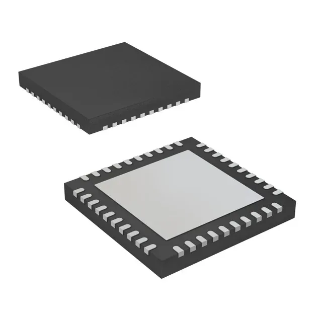
What this clock buffer does for your clock tree
The LMK00308SQE/NOPB is a 3:9 fanout buffer, multiplexer, and level translator from Texas Instruments, built for distributing high-speed reference clocks in systems that mix CML, HCSL, HSTL, LVDS, LVPECL, SSTL, or crystal inputs. It handles a maximum frequency of 3.1 GHz, which covers PCIe Gen4/5 reference clocks, 10G Ethernet, and JESD204B SYSREF distribution without needing a separate translation stage. The 3:1 input mux lets a single device select among three clock sources — useful for redundant oscillator inputs or switching between a local crystal and a backplane-derived clock. The nine outputs can be individually configured as HCSL, LVCMOS, LVDS, or LVPECL, so one part feeds SerDes, FPGA banks, and logic with different logic families.
Supply rail tolerance and temperature grade
The supply voltage range is 3.15 V to 3.45 V — a tight 3.3 V nominal with only ±150 mV margin. The board's 3.3 V regulator must hold within this window under load; a 3.3 V rail that droops to 3.0 V at full fanout will violate the minimum.
It is ROHS3 compliant.