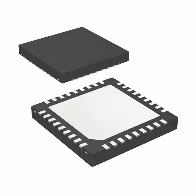
Device identity and signal-format reach
The Texas Instruments LMK00306SQX/NOPB is a fanout buffer, distribution, multiplexer, and translator in one device — it accepts a single clock source and distributes up to seven copies across different logic families. The 3:7 input-to-output ratio means three selectable inputs feed seven outputs, giving the system architect flexibility to route a reference clock to multiple loads without adding separate fanout trees. Input compatibility spans CML, HCSL, HSTL, LVDS, LVPECL, SSTL, and crystal — the widest signal-format set in this class. Outputs are available in HCSL, LVCMOS, LVDS, and LVPECL, so the same buffer can drive a PLL reference, a SerDes reference, and a logic clock from one input without external level translators.
Frequency ceiling and differential path
Rated for 3.1 GHz maximum frequency, the LMK00306SQX/NOPB covers the full range of high-speed serial standards — PCIe Gen4/5 reference clocks, 10G Ethernet, and JESD204B SYSREF. The differential input-to-output path is maintained throughout (Yes/Yes), so the signal integrity of a 100 MHz LVDS oscillator or a 312.5 MHz LVPECL SerDes reference is preserved without single-ended conversion loss.
Package footprint and PCB layout
The tape-and-reel packaging is the standard ordering code for automated assembly. The /NOPB suffix indicates lead-free / RoHS-compliant finish — no additional Pb-free qualification step is needed for the reflow profile.