What the 3000 V/µs slew rate means for your signal chain
The LM6172IN/NOPB is a dual voltage feedback amplifier from Texas Instruments. Its headline 3000 V/µs slew rate means the output can swing 10 V in about 3.3 ns — fast enough to reproduce a 5 MHz square wave with minimal edge distortion, or to settle a large-signal pulse before the next sample arrives in a high-speed ADC driver stage.
Bandwidth and gain: matching the loop to the signal
The -3 dB bandwidth is 160 MHz, and the gain-bandwidth product is 100 MHz. At a closed-loop gain of 10, the usable signal bandwidth is about 10 MHz before the open-loop roll-off cuts in — a practical ceiling for video distribution or high-speed data acquisition front-ends. Supply span runs from 5.5 V minimum to 36 V maximum, so the part works on a single 5 V rail (with headroom) or on ±15 V supplies common in industrial analog systems. Each channel draws 4.6 mA quiescent, keeping the total for both channels under 10 mA. Input offset voltage is 400 µV typical, and input bias current is 1.2 µA — both moderate figures that suit a general-purpose signal path but may need a trim or a lower-bias part for a high-impedance sensor front-end. Output current capability is 90 mA per channel, enough to drive a 50-ohm back-terminated cable or a moderate capacitive load without an external buffer.
Through-hole DIP: board integration and thermal story
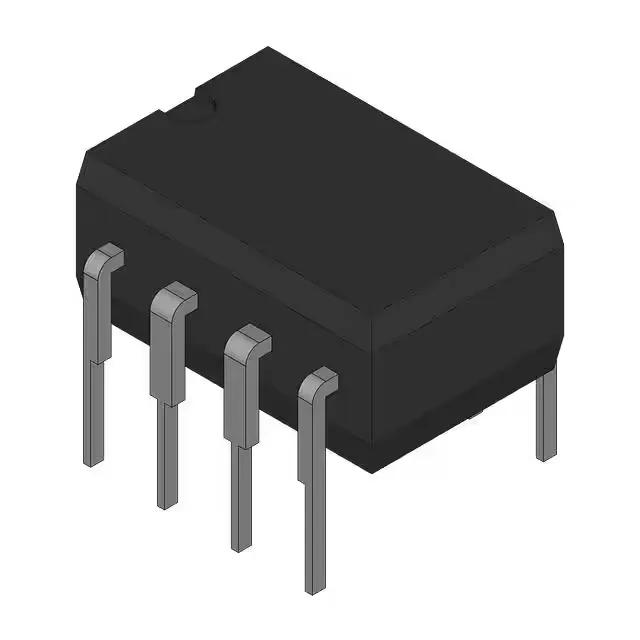
The 8-pin DIP package (0.300" body width, 2.54 mm pitch) is a through-hole footprint that mates with standard breadboards, prototyping sockets, and legacy PCB layouts. The 8-PDIP supplier package code confirms the same mechanical outline. No exposed pad — heat dissipates through the leads into the copper pour; for continuous high-slew-rate operation, a short lead length and a ground-plane via under the body help keep junction temperature inside the -40°C to 85°C ambient range.