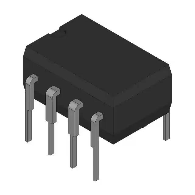
Package and board integration — 8-DIP through hole
The LF411CP ships in a tube of 8-DIP (0.300", 7.62mm) packages, mounting through hole on a standard 0.100-inch pitch socket or soldered directly into plated through holes. The 8-PDIP supplier package designation matches the industry-standard DIP-8 footprint, so a single board layout serves multiple second-source JFET op-amps in the same outline.
What the key ratings mean for your signal chain
The J-FET input stage delivers 50 pA typical input bias current — three orders of magnitude lower than a bipolar-input op-amp. For a photodiode or high-impedance sensor front-end, this bias current translates into a DC offset error across the source resistance that is negligible at 50 pA but doubles every 10°C, so budget the 70°C upper limit into the error analysis. A 13V/µs slew rate means the output can swing 10 V peak-to-peak in about 770 ns, supporting full-power bandwidth up to roughly 200 kHz without slew-rate limiting. The 3 MHz gain-bandwidth product sets the small-signal closed-loop bandwidth — at a gain of 10, the -3 dB point is 300 kHz, adequate for audio, instrumentation, and control loops that do not need video-speed settling. Supply span from 7 V to 36 V covers both single-supply (5 V to 30 V with headroom) and split-supply (±3.5 V to ±18 V) rails. The 2 mA typical supply current per amplifier keeps the thermal budget low in multi-channel boards — eight amplifiers draw 16 mA, well within the capacity of a 78L05 regulator.
Where this op-amp class fits in a design
JFET-input op-amps like the LF411 are specified wherever the source impedance is high enough that a bipolar input stage's bias current would create an unacceptable voltage error. Typical applications include photodiode transimpedance amplifiers, pH probe buffers, piezoelectric sensor conditioners, and active filters where input bias current dominates the DC drift. The commercial temperature grade (0°C to 70°C) limits it to indoor, temperature-controlled environments — it is not rated for automotive under-hood or industrial outdoor deployment without qualification testing.