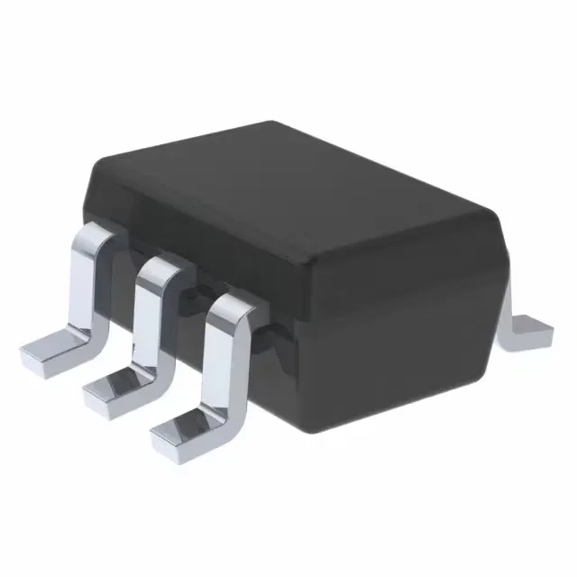
Package and board integration
The INA212AIDCKT ships in a 6-lead SC-70-6 package, also described as 6-TSSOP/SC-88/SOT-363 — a 2.0 mm × 1.25 mm body with 0.65 mm pin pitch. The SC-70-6 footprint lands directly on a two-layer board; no thermal pad or exposed paddle to plan for. The narrow pitch means the shunt resistor and sense traces should route to the input pins with matched Kelvin connections to keep the input offset voltage from coupling into the measurement.
What the key ratings mean for a shunt-based measurement
The 4 kHz gain-bandwidth product sets the usable measurement bandwidth — above 4 kHz the closed-loop gain rolls off at 20 dB/decade, so a 100 kHz ripple current on the shunt produces less than 1/25th of the DC gain. The 0.4 V/µs slew rate limits the large-signal edge response; for a 1 V step at the output the rise time is roughly 2.5 µs, which matters if the downstream ADC samples during a current transient. Input offset voltage is 0.55 µV typical — this is the DC error at zero current. The 28 µA input bias current flows into the shunt resistor; with a 10 mΩ shunt the bias adds 0.28 µV of additional offset — negligible for most designs but relevant for sub-milliohm shunts. The 65 µA quiescent current makes it suitable for always-on current monitoring in battery-powered equipment.