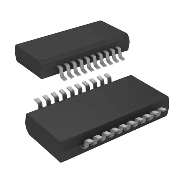
20-SSOP footprint and what it demands of the board
The CY74FCT2541TQCT comes in a 20-SSOP package with a 0.154-inch body width and 3.90 mm body width — a standard fine-pitch SOIC variant that places well on a two-layer board without micro-vias. The 1.27 mm lead pitch gives the pick-and-place a forgiving target; tombstoning risk is low with the 15 mA / 12 mA output drive not pulling enough current to heat the package unevenly during reflow. MSL is not explicitly stated in the record, but the package is a molded SSOP — typical MSL-1 or MSL-2 for this family. If the reel has been opened and the floor life is uncertain, a 24-hour bake at 125°C before reflow is cheap insurance against popcorning.
Supply rails and temperature — where this fits on the board
The 4.75 V to 5.25 V supply range ties it to a 5 V nominal rail — the same bus that powers legacy TTL and 5 V CMOS logic. It will not work on a 3.3 V or lower supply without a level translator at the input. The -40°C to 85°C operating temperature range covers industrial enclosures, outdoor telecom cabinets, and unheated factory floors.
Output drive — what 15 mA / 12 mA means for fan-out
The 15 mA source and 12 mA sink capability at the output is modest by today's 24 mA or 32 mA bus-driver standards. Driving a 50 pF load at 5 V, the output transition time will be around 4–6 ns — fine for a 20–30 MHz clocked bus, but marginal for a 50 MHz+ backplane without a dedicated line driver. The 3-state output allows multiple buffers to share a common data bus — the high-impedance state presents a 10 µA max leakage load to the bus, so 8 to 12 of these can be paralleled without exceeding the bus pull-up current budget.
Lifecycle and sourcing — active part, quoted to order
ROHS3 compliant — the part is lead-free and compatible with standard Pb-free reflow profiles (260°C peak).