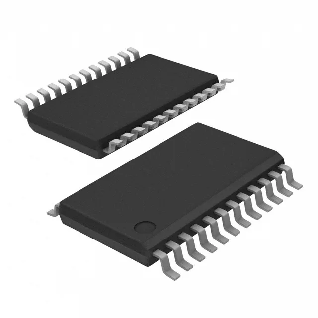
230 MHz PLL synthesizer with 1:9 LVCMOS fan-out
The Texas Instruments CDCEL949PWRG4 is a clock/frequency synthesizer built around a PLL that can be bypassed for a clean reference path. It accepts an LVCMOS or crystal input and delivers up to nine LVCMOS outputs, each capable of running up to 230 MHz. The 1:9 ratio means a single reference clock fans out to nine loads — useful for distributing a master clock across multiple ASICs, FPGAs, or PHYs on the same board without adding separate buffers.
The supply range is 1.7V to 1.9V, which centres on a 1.8V rail. If the board already carries a 1.8V LDO or switcher, this part drops in without a new regulator. If the closest rail is 3.3V or 2.5V, a dedicated 1.8V supply is needed — factor in the extra component cost and board area. The narrow tolerance (200 mV window) also means the supply must be well-regulated; a noisy rail can couple into the PLL and degrade jitter performance.
Industrial temperature grade and 24-TSSOP footprint
The 24-TSSOP package (4.40 mm wide, 0.65 mm pitch) is a common footprint that routes easily on a two-layer board for the clock fan-out traces. The PLL bypass feature is useful during board bring-up or when the application needs a jitter-free reference — the PLL can be disabled and the input passed straight to the outputs.
That said, the narrow supply rail and 24-TSSOP package limit drop-in alternatives — if the board layout is locked, a future EOL would require a board spin.