230 MHz synthesizer with 1:7 fanout on a 1.8V rail
The Texas Instruments CDCEL937PWRG4 is a clock/frequency synthesizer that takes a single LVCMOS or crystal input and distributes it across seven LVCMOS outputs at up to 230 MHz. The on-chip PLL includes a bypass mode, letting the design switch between a clean synthesised clock and a direct reference feed without an external mux.
The PLL-with-bypass architecture means the device can generate a multiplied/cleaned clock from a lower-frequency crystal or pass through an external reference with the PLL disabled. This is useful during system test or when the board needs to synchronise to an external clock source without the PLL jitter. One input drives seven outputs. That 1:7 ratio eliminates a separate clock fanout buffer — the synthesizer and the distribution happen in one 20-pin TSSOP package, saving board area and reducing the BOM line count. All I/O are LVCMOS — no differential signalling. The outputs are single-ended, so the fan-out traces need impedance-matched routing if the clock edges are fast enough to cause reflections above a few centimetres.
20-TSSOP footprint and supply reality
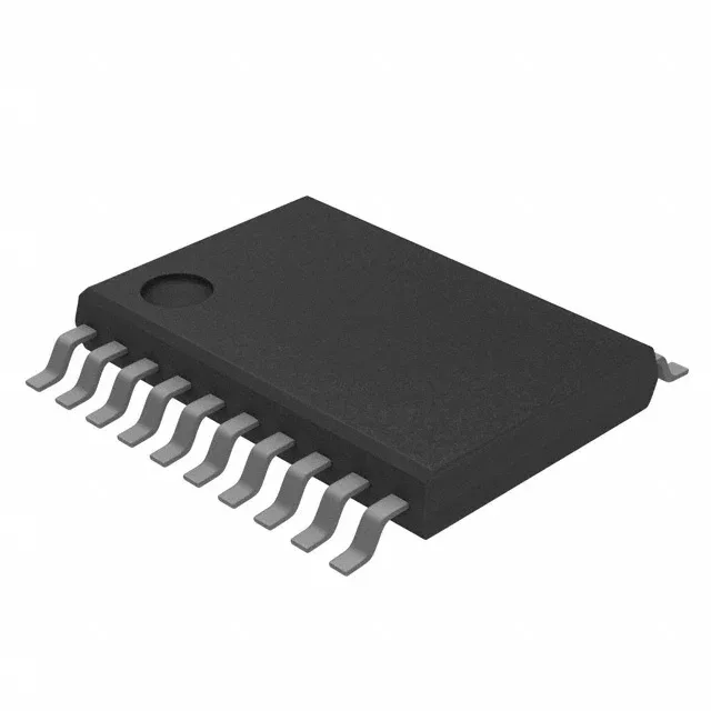
The package is 20-TSSOP, 4.40 mm wide.