PLL clock generator with bypass — one input, nine outputs
The Texas Instruments CDCE949PWRG4 is a PLL-based clock generator that accepts an LVCMOS or crystal reference on its single input and delivers up to nine LVCMOS clock outputs, each programmable through the on-chip dividers. The PLL includes a bypass mode, which lets the reference clock pass through unmodified when jitter performance or a clean system clock is the priority. Maximum output frequency reaches 230 MHz, covering common Ethernet, FPGA, and processor reference clock rates.
Supply and temperature — narrow rail, industrial range
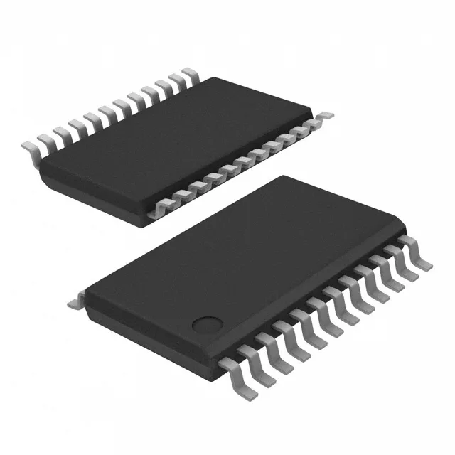
Package and footprint — 24-TSSOP on 0.65 mm pitch
The 4.40 mm body width keeps the footprint compact.