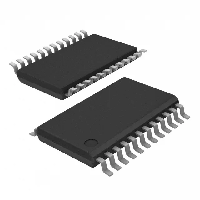
Texas Instruments CDCE949PWG4 — Clock & Timing ICs

CDCE949PWG4 PLL Clock Generator, 230 MHz, 1.7-1.9V, 24-TSSOP

MPNCDCE949PWG4
End of Life

Texas Instruments CDCE949PWG4 PLL Clock Generator, PLL Yes with Bypass, 230 MHz max, 1.7V-1.9V supply, 1:9 input:output, LVCMOS I/O, 24-TSSOP, -40°C to 85°C.

$118.8000Ref. price · indicative, final on quote
Independent supplier — new & surplus stockAuthenticity-screened · ESD-safe packingListing updated Aug 2026

Specifications

CDCE949PWG4 specifications
ParameterValue
TypePLL Clock Generator
MountingSurface Mount
Supply voltage1.7V ~ 1.9V
Frequency - max230MHz
Operating temperature-40°C~85°C
PLLYes with Bypass
InputLVCMOS, Crystal
OutputLVCMOS
PackageTube
Case24-TSSOP (0.173\", 4.40mm Width)
Divider (Multiplier)Yes/No
Number of circuits1
Ratio - Input:Output1:9
Differential - Input:OutputNo/No

Product details

230 MHz PLL clock fanout in a 24-TSSOP

The integrated PLL supports frequency synthesis and jitter attenuation; a bypass mode lets the reference clock pass through unmodified when the PLL is not needed. It operates from a 1.7V to 1.9V supply rail, which ties it to the core voltage plane of low-power ASICs, FPGAs, or SoCs rather than a 3.3V or 2.5V I/O rail.

Supply rail and temperature grade — fit for industrial base stations

The 1.7V to 1.9V supply range is narrow and low — this part is designed for the core supply of a digital processor or FPGA, not a general-purpose 3.3V clock buffer.

Frequently asked questions

What is the maximum frequency of CDCE949PWG4?

The maximum output frequency is 230 MHz on each of the nine LVCMOS outputs. This ceiling is set by the PLL VCO range and the output divider network.