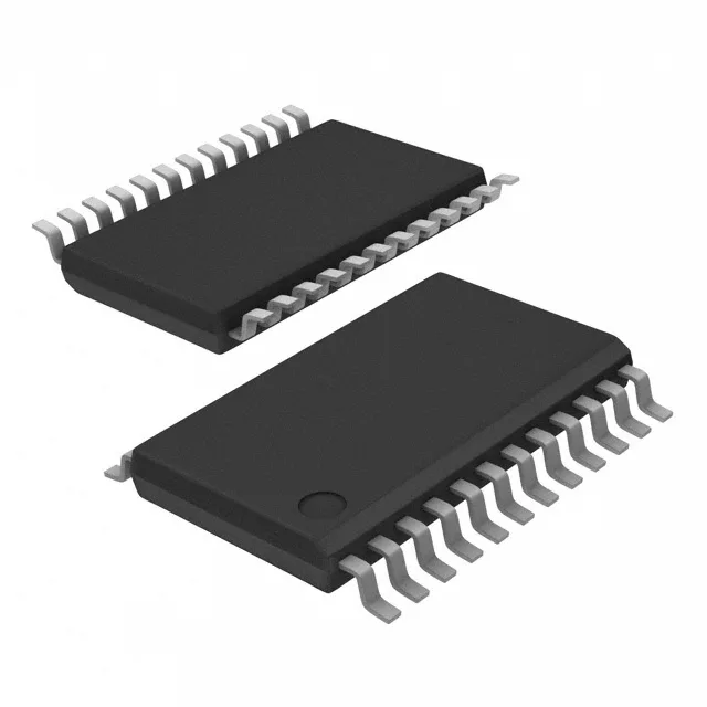
Four-PLL clock generator for low-voltage timing trees
The Texas Instruments CDCE949PW is a 4-PLL VCXO clock generator in a 24-TSSOP package, designed to synthesize and distribute clean clock signals from an LVCMOS or crystal input. It delivers up to nine LVCMOS outputs from a single reference, with the PLLs individually configurable and bypassable when you need a clean feed-through path. The 230 MHz maximum output frequency covers most processor, FPGA, and serial-interface clocking needs, and the 1.7V to 1.9V supply rail fits the sub-2V core voltages common in modern digital ASICs and SoCs.
230 MHz ceiling and the 1:9 fan-out
The 230 MHz maximum frequency is the hard limit for any output — if your design needs a 250 MHz reference for a SerDes or a high-speed ADC, this part won't close timing. The 1:9 input-to-output ratio means one crystal or reference oscillator can feed nine clock loads, which saves a separate buffer stage on the board. All I/O is single-ended LVCMOS; there are no differential outputs (LVPECL, LVDS), so for a pair of differential clock trees you would need an external fanout buffer after this device.
Supply and temperature — the deployment envelope
The 1.7V to 1.9V supply range is tight — this is not a 3.3V or 2.5V part, so a separate 1.8V rail (or an LDO from a higher bus) is mandatory. The 24-TSSOP package is a standard 4.4 mm wide body with 0.65 mm pitch — a common footprint that rework stations handle easily with a hot-air nozzle.
The ROHS3 compliance is current, so no end-of-life exemption paperwork is needed.