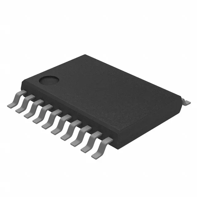
Texas Instruments CDCE937PWRG4 — Clock & Timing ICs

Texas Instruments CDCE937PWRG4 PLL Clock Generator, 230 MHz

MPNCDCE937PWRG4
End of Life

Texas Instruments CDCE937PWRG4, PLL Clock Generator, 230 MHz max, 1.7V–1.9V supply, LVCMOS/Crystal input, LVCMOS output, 1:7 ratio, 20-TSSOP, -40°C~85°C.

$3.3500Ref. price · indicative, final on quote
Sourced new & surplus through independent channelsAuthenticity-screened · ESD-safe packingListing updated Aug 2026

Specifications

CDCE937PWRG4 specifications
ParameterValue
TypePLL Clock Generator
MountingSurface Mount
Voltage1.7V ~ 1.9V
Frequency230MHz
Operating temperature-40°C~85°C
PLLYes with Bypass
InputLVCMOS, Crystal
OutputLVCMOS
PackageTape & Reel (TR)
Case20-TSSOP (0.173\", 4.40mm Width)
Divider (Multiplier)Yes/No
Number of circuits1
Ratio - Input:Output1:7
Differential - Input:OutputNo/No

Product details

PLL clock generator with bypass — what the 1:7 ratio buys you

The Texas Instruments CDCE937PWRG4 is a PLL clock generator that accepts either an LVCMOS or crystal reference and produces up to seven LVCMOS clock outputs, each programmable up to 230 MHz. The integrated PLL includes a bypass path — when bypassed, the input clock passes through with minimal added jitter, useful for system test modes or low-latency paths. The 1:7 input-to-output ratio means a single reference can feed multiple clock domains, reducing the external oscillator count on the board.

Supply rail and temperature — design constraints

The device operates from a 1.7V to 1.9V supply, which aligns with 1.8V logic families common in low-power FPGAs, SoCs, and memory interfaces. The 20-TSSOP package (4.40 mm width) is a fine-pitch surface-mount footprint; verify the land pattern matches the supplier device package drawing before layout.

Frequently asked questions

Is CDCE937PWRG4 compatible with a 1.8V LVCMOS input?

Yes. The device accepts LVCMOS inputs and its supply range of 1.7V to 1.9V directly covers the 1.8V LVCMOS logic level. The input threshold scales with the supply, so a 1.8V LVCMOS signal is within the guaranteed VIH/VIL window.

What is the maximum output frequency of CDCE937PWRG4?

The maximum output frequency is 230 MHz. This ceiling applies to any of the seven LVCMOS outputs when the PLL is engaged. The bypass path passes the input frequency directly without multiplication.