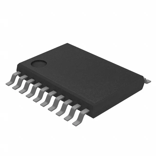
Texas Instruments CDCE906PW — Clock & Timing ICs

CDCE906PW PLL Frequency Synthesizer, 167 MHz, 20-TSSOP

MPNCDCE906PW
Active

Texas Instruments CDCE906PW PLL Frequency Synthesizer, 167 MHz max, 1:6 LVCMOS fan-out, PLL with bypass, 3V–3.6V supply, 20-TSSOP, 0°C to 70°C.

$6.5300Ref. price · indicative, final on quote
Independent supplier — new & surplus stockAuthenticity-screened · ESD-safe packingListing updated Aug 2026

Specifications

CDCE906PW specifications
ParameterValue
TypePLL Frequency Synthesizer
MountingSurface Mount
Supply voltage3V ~ 3.6V
Frequency - max167MHz
Operating temperature0°C~70°C
PLLYes with Bypass
InputLVCMOS, Crystal
OutputLVCMOS
PackageTube
Case20-TSSOP (0.173\", 4.40mm Width)
Divider (Multiplier)Yes/Yes
Number of circuits1
Ratio - Input:Output1:6
Differential - Input:OutputYes/No

Product details

PLL frequency synthesizer with 1:6 fan-out

The Texas Instruments CDCE906PW is a PLL frequency synthesizer that accepts LVCMOS or crystal inputs and delivers six LVCMOS outputs, each programmable up to 167 MHz. The integrated PLL includes a bypass mode, letting the designer pass a clean reference clock straight through when synthesis is not needed.

167 MHz ceiling and 1:6 ratio — clock tree planning

The 167 MHz maximum output frequency covers most common system clocks — Ethernet MACs, FPGAs, SoC reference inputs — without needing a higher-speed PLL. The 1:6 input-to-output ratio means a single reference oscillator can feed six clock domains, reducing BOM oscillator count and board area.

Runs from 3.0 V to 3.6 V, matching the 3.3 V rail common in digital systems.

Housed in a 20-TSSOP (4.40 mm width) surface-mount package. The 0.65 mm pitch is layout-friendly on two-layer boards; the small body saves space on dense mixed-signal cards.

Frequently asked questions

What is the difference between CDCE906PW and CDCE906PWR?

The CDCE906PW ships in a Tube; the CDCE906PWR ships in Tape & Reel. The silicon and package are identical.

What is the CDCE906PW's maximum output frequency?

The CDCE906PW can generate LVCMOS outputs up to 167 MHz.

Does the CDCE906PW support a bypass mode?

Yes, the PLL includes a bypass mode, allowing the input reference clock to pass directly to the outputs without frequency synthesis.