Clock-tree workhorse with spread-spectrum and PLL bypass
The Texas Instruments CDCE706PWRG4 is a spread-spectrum clock driver that accepts a single LVCMOS or crystal input and fans it out to six LVCMOS outputs. A PLL with bypass mode lets you either clean up a jittery reference or pass through a clean clock unmodified — the bypass path is the one to use when the input clock is already within tolerance and you just need the fanout. Maximum output frequency is 300 MHz, which covers the vast majority of digital clock trees in networking, industrial control, and test equipment. The 1:6 fanout ratio means a single device can feed six clock domains — a design needing more than six outputs will require a second stage or a different part.
Supply rail and temperature grade — the operating envelope
The supply range is 3.0 V to 3.6 V, so this part runs on a nominal 3.3 V rail.
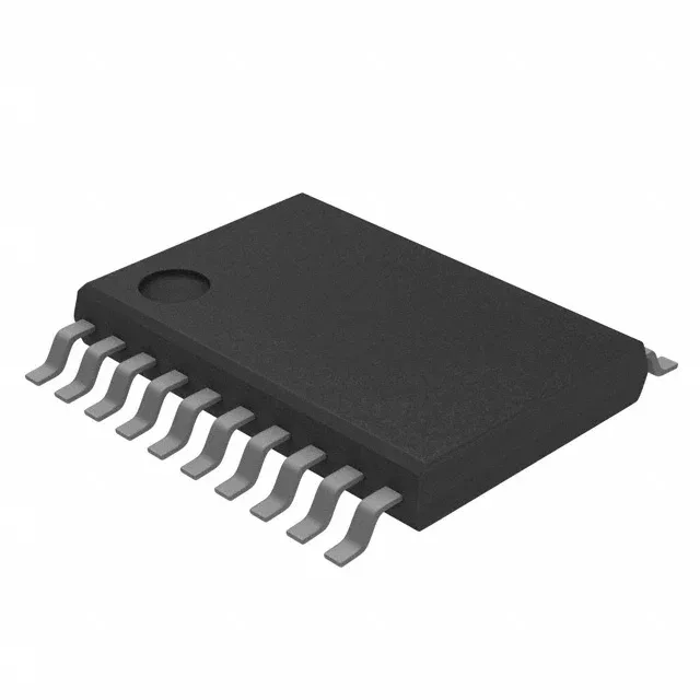
20-TSSOP package — footprint and layout
This is a surface-mount package with 0.65 mm pitch — a standard 2-layer board can route the fanout traces, but keeping the clock traces impedance-controlled and isolated from noisy supply lines is the usual layout discipline. The supplier device package is 20-TSSOP, matching the package/case field.