Spread spectrum clock distribution — what the ratings mean
The CDCE706PWG4 is a spread spectrum clock driver, meaning it modulates the output clock frequency within a controlled band to reduce peak electromagnetic emissions. This makes it a direct fit for EMI-sensitive designs — LCD panels, set-top boxes, networking equipment, and any board that must pass radiated emissions testing without a metal shield. Maximum output frequency is 300 MHz, which sets the ceiling for the clock tree. The 1:6 fanout ratio means one input (LVCMOS or crystal) drives six LVCMOS outputs — enough for a typical SoC plus its peripheral clock domains without an additional buffer. The integrated PLL includes a bypass mode (PLL Yes with Bypass), allowing the input reference to pass through unmodified for test modes or low-jitter paths where spread spectrum is not desired. The divider and multiplier are both programmable, so a single 25 MHz or 27 MHz crystal can generate multiple output frequencies across the 300 MHz range.
Supply and temperature grade
The input stage accepts both LVCMOS and crystal sources, while the output is LVCMOS. The differential input option (Differential - Input:Output Yes/No) means a clean differential clock from an oscillator or another PLL can feed the device, with the outputs remaining single-ended LVCMOS.
20-TSSOP package — board-fit note
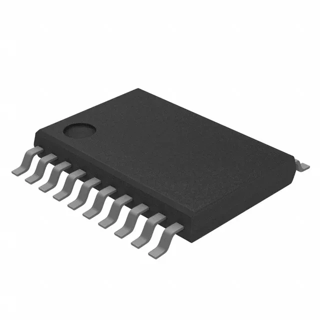
Housed in a 20-pin TSSOP with 4.40 mm body width (EIAJ standard). The 0.65 mm pin pitch is layout-friendly — two-layer boards can route the six outputs and supply traces without blind vias. The surface-mount package is supplied in tube (: Package Tube), though reel options may be available through distribution.