Texas Instruments CDCE6214RGET — Clock & Timing ICs

TI CDCE6214RGET Clock Generator, PLL, 350 MHz, 24-VFQFN

MPNCDCE6214RGET
Active

Texas Instruments CDCE6214RGET Clock Generator, PLL Yes, 350 MHz max, 2:4 Input:Output, Differential or Single-Ended Input, LP-HCSL, LVCMOS, LVDS Output, 24-VFQFN Exposed Pad, -40°C to 85°C.

$6.3600Ref. price · indicative, final on quote
Independent supplier — new & surplus stockAuthenticity-screened · ESD-safe packingListing updated Aug 2026

Specifications

CDCE6214RGET specifications
ParameterValue
TypeClock Generator
MountingSurface Mount, Wettable Flank
Supply voltage1.71V ~ 3.465V
Frequency - max350MHz
Operating temperature-40°C~85°C
PLLYes
InputDifferential or Single-Ended
OutputLP-HCSL, LVCMOS, LVDS
PackageTape & Reel (TR); Cut Tape (CT)
Case24-VFQFN Exposed Pad
Divider (Multiplier)Yes/No
Number of circuits1
Ratio - Input:Output2:4
Differential - Input:OutputYes/Yes

Product details

What the 350 MHz PLL clock generator actually does on your board

The CDCE6214RGET: This is a single-circuit clock generator with an integrated PLL that synthesizes a clean output clock from a differential or single-ended reference. The 350 MHz ceiling means it covers PCIe Gen3/4 reference clocks, 10G Ethernet, and most SERDES applications that need a low-jitter source in that band. The 2:4 input-to-output ratio lets it fan out one reference to four independent clock domains, each programmable to LP-HCSL, LVCMOS, or LVDS levels — so a single IC can feed a mix of logic, SerDes, and RF blocks without external level translators.

Package note for the rework bench

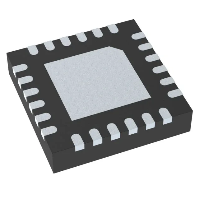
Housed in a 24-VFQFN with exposed pad and wettable flank terminals. The wettable flank means the solder joints are visually inspectable after reflow — the side of the pad wets up and you can see the fillet, which eliminates the X-ray-only guesswork on QFNs.

Frequently asked questions

What output formats does the CDCE6214RGET support?

It outputs LP-HCSL, LVCMOS, or LVDS. That covers PCIe reference clocks (HCSL), general-purpose logic (LVCMOS), and high-speed SerDes interfaces (LVDS) from a single device.

What is the maximum output frequency of this part?

350 MHz. That is the upper limit for the PLL and output divider — useful for PCIe Gen4 (100 MHz reference), 10G Ethernet (156.25 MHz), or any clock tree needing a clean source up to that speed.