1.2 GHz PLL clock generator — what the 1:1 ratio buys you
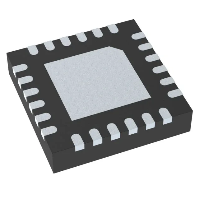
The CDCE421ARGER is a single-circuit PLL clock generator from Texas Instruments that takes an LVCMOS or crystal reference and delivers a differential LVDS or LVPECL output up to 1.2 GHz. The 1:1 input-to-output ratio means the PLL multiplies or divides the reference in a single stage — no cascaded synthesis — which keeps jitter lower than a multi-PLL chain. The 24-VQFN (4x4 mm) exposed-pad package helps pull heat out of the die when the output is driving a long backplane trace or a high-speed SERDES reference.
Differential output standards — LVDS vs LVPECL
The part outputs both LVDS and LVPECL, which covers the two dominant differential signalling levels for FPGA and ASIC reference clocks. LVDS swings about 350 mV centred on 1.2 V common mode; LVPECL swings about 800 mV centred on 2 V. The choice determines the AC-coupling capacitor value and the termination network — LVDS terminates with 100 Ω across the pair, LVPECL needs a Thevenin equivalent to VCC – 2 V. If the downstream receiver expects CML, an external level shifter is needed.
Dropping below 3.15 V may reduce the output swing margin at 1.2 GHz — keep the supply within 3.3 V ±5 % for full performance.