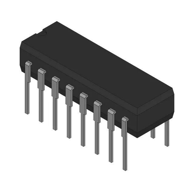
1K x 1 parallel SRAM for high-reliability designs
The 93425DMQB40 is a 1Kbit parallel SRAM organized as 1K x 1 bit, with a 30 ns access time and a 20 ns write cycle.
If your memory controller or FPGA interface has a 33 MHz or slower bus clock (30 ns period), this part can be used without wait states. At higher bus speeds, the controller must insert wait cycles, which reduces throughput. The 20 ns write cycle time is similarly tight — the write pulse width must be held for at least 20 ns to guarantee data capture. For a design engineer, this means verifying the setup/hold timing against the controller's AC specs is essential before committing the BOM.
Through-hole package and military temperature grade
This part is a through-hole device, which means it is intended for boards where the memory is socketed or hand-soldered — typical in high-reliability modules and prototype runs. For a rework tech, this means the part can survive the thermal cycling of a hot-air rework station, but the board should be preheated to avoid thermal shock. The 4.5 V supply is a single fixed rail; the design must provide a clean 4.5 V ±5% or better, as the part does not have a wide supply range.