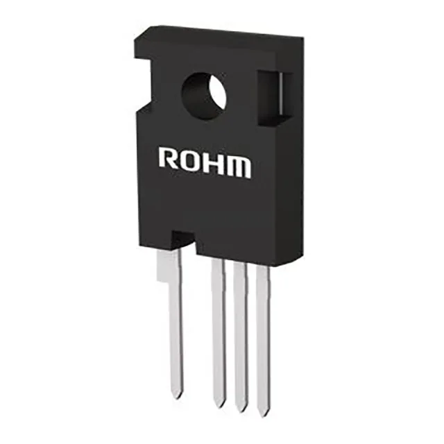
750 V SiCFET for high-efficiency power switching
Built on a trench SiC structure, it delivers a typical on-resistance of 59 mOhm at 17 A with an 18 V gate drive. With a maximum junction temperature of 175°C, it is suited for power conversion stages where efficiency and thermal margin are critical — think switch-mode power supplies, EV onboard chargers, photovoltaic inverters, and industrial motor drives.
The 750 V Vdss rating gives you a solid margin for 400 V bus architectures common in three-phase industrial and automotive systems. The 59 mOhm Rds(on) at 18 V gate drive sets the conduction loss budget — at 17 A, expect about 17 W dissipation in the channel alone, which the TO-263-7L package can handle with proper PCB copper and thermal vias. Gate charge of 63 nC at 18 V means the gate driver needs to source and sink that charge each switching cycle; a driver with 2 A peak current capability will keep switching losses manageable at frequencies up to 100 kHz or so. Input capacitance of 1460 pF at 500 V Vds is moderate for a SiC device, so the driver sees a capacitive load that rises with voltage — factor that into your gate-drive loop layout.
Package and thermal: TO-263-7L surface-mount
The TO-263-7L (D²PAK) package is a surface-mount power package with a large exposed metal tab on the bottom. The 93 W maximum power dissipation assumes the tab is soldered to a suitable heatsink area — without that, derate aggressively.
No last-time-buy risk or obsolescence concern on this one.