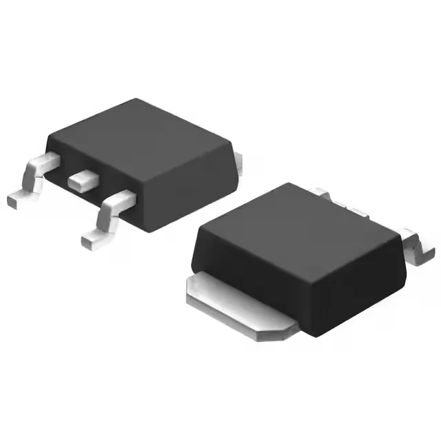
650 V N-Channel MOSFET — switching-stage fit
The R6504KND3TL1: The 650 V Vdss rating puts it squarely into off-line power supplies, PFC boost stages, and flyback converters where the DC bus sits at 380-400 V and the reflected voltage can push past 600 V.
Rds(on) and gate drive — what the numbers mean for the BOM
At the full 4 A rating, conduction loss is roughly 6.3 W — the TO-252 package can dissipate up to 58 W at the case, so the real limit is the PCB copper area and ambient airflow, not the silicon. Gate charge is 10 nC at 10 V, which keeps switching losses low enough that a simple gate-driver IC or even a discrete totem-pole can drive it into the 50-100 kHz range without excessive driver dissipation.
Supplied in the TO-252-3 (DPak) surface-mount package, also known as SC-63. The exposed tab is the drain — it must be soldered to a sufficient copper area on the PCB to carry the heat. The 270 pF input capacitance at 25 V drain bias means the gate-drive impedance should be low enough to avoid Miller-induced turn-on at high dV/dt edges.