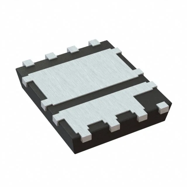
Dual die in one package — the parametric split matters
The HP8K24TB packs two independent N-channel MOSFETs into a single 8-PowerTDFN package, but the two halves are not identical.
Current rating depends on where you pull the heat
The 80 A continuous drain current (Tc) for the higher-rated die assumes the case temperature is held at 25°C — realistic only with a good thermal path to the board or a heatsink on the exposed pad. At ambient (Ta) the same die is derated to 26 A. The 3 W maximum power dissipation at Ta means the total copper area under the 8-HSOP pad and the number of vias to the inner ground plane set the real-world current ceiling.
Gate charge and switching speed
Gate charge (Qg) at 10 V is 10 nC for the lower-current die and 36 nC for the higher-current die. The difference reflects the larger gate area of the 3 mOhm device. A gate driver sourcing 1 A can switch the bigger die in about 36 ns, but the total drive current at a given frequency is the sum of both gates if they switch simultaneously — budget for 46 nC total per cycle.