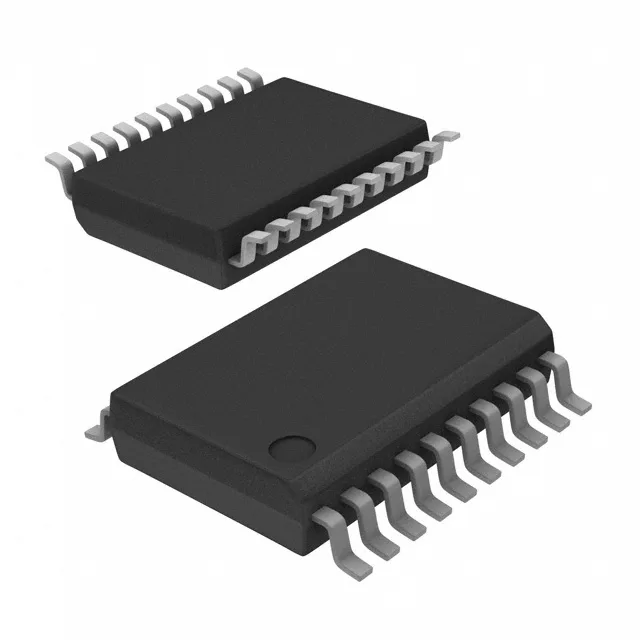
ROHM Semiconductor BM60059FV-CE2 — Power Management (PMIC / Gate Driver)

ROHM BM60059FV-CE2 isolated gate driver, 2500Vrms, 1A peak

MPNBM60059FV-CE2
End of Life

ROHM BM60059FV-CE2, single-channel digital isolator with integrated gate driver, magnetic coupling, 2500Vrms isolation, 1A peak output, 100kV/µs CMTI, 28-SSOP package, -40°C to 125°C.

$8.72Ref. price · indicative, final on quote
Packaging28-SSOP (0.315", 8.00mm Width)
RoHSROHS3 Compliant
Independent supplier — new & surplus stockAuthenticity-screened · ESD-safe packingListing updated Jul 2026

Specifications

BM60059FV-CE2 specifications
ParameterValue
MountingSurface Mount
Voltage - isolation2500Vrms
Voltage - output supply4.5V ~ 24V
Current - peak output1A
Current - output high, low40µA, 160µA
Operating temperature-40°C ~ 125°C
Pulse width distortion400ns
Approval agencyUL
PackageTape & Reel (TR); Cut Tape (CT)
TechnologyMagnetic Coupling
Case28-SSOP (0.315\", 8.00mm Width)
Channels1
Propagation delay tpLH (tpHL)450ns, 450ns
Common mode transient immunity100kV/µs

Product details

What this isolated gate driver brings to a power stage

The ROHM BM60059FV-CE2 is a single-channel digital isolator with a built-in gate driver, using magnetic coupling to deliver 2500Vrms of galvanic isolation between the logic-side input and the power-stage output. It is designed to drive the gate of a power MOSFET, IGBT, or SiC MOSFET directly, with a peak output current rating of 1A.

Propagation delay and pulse-width distortion — timing budget for dead-time

The maximum propagation delay from input to output is 450ns for both rising and falling edges (tpLH / tpHL). Pulse-width distortion is capped at 400ns maximum. In a half-bridge or full-bridge topology, these numbers set the lower bound on the dead-time you need to program into the controller — if you try to run dead-time below the PWD spec, you risk shoot-through on one switching cycle. The 1A peak output is enough to drive the gate charge of a typical SiC MOSFET or medium-current IGBT through the Miller plateau without excessive switching loss, but the 450ns delay means the dead-time budget will be in the hundreds of nanoseconds, not single-digit nanoseconds.

At the low end, a 5V rail drives the gate of a logic-level MOSFET; at 24V, the same part drives a standard IGBT or a SiC MOSFET that needs a +15V to +20V gate drive. The 1A peak output current is a typical figure — enough to charge the gate capacitance quickly, but not a high-current driver for paralleled modules. The high-side and low-side output currents (40µA and 160µA respectively) are the static drive levels, not the switching peak; the 1A peak is what matters for the turn-on and turn-off edges.

Frequently asked questions

Can BM60059FV-CE2 drive SiC MOSFETs?

The 1A peak output current and 100kV/µs CMTI make it suitable for driving SiC MOSFETs in many designs, provided the gate charge of the specific SiC device does not exceed what the driver can deliver within the switching period. The 4.5V to 24V output supply range covers the typical +15V to +18V gate drive voltage for SiC parts. The 450ns propagation delay means the dead-time budget must account for that latency — it will not match a sub-100ns driver.

What is the CMTI of BM60059FV-CE2?

The minimum common-mode transient immunity is 100kV/µs. This is the key specification for fast-switching power stages — it tells you the driver will not latch or mis-fire when the half-bridge midpoint slews at high dV/dt, which is typical in SiC and GaN designs.