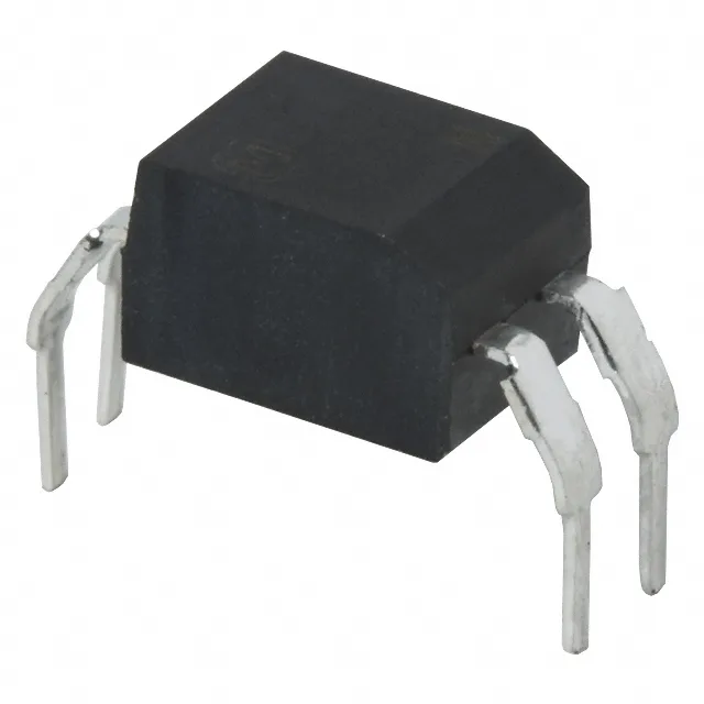
The FOD817BW: Sourced through independent distribution against an RFQ.
Isolation and CTR — the two fit dimensions
Rated for 5000Vrms isolation — this is the withstand voltage between input LED and output phototransistor, tested per the optocoupler safety standard. Suitable for reinforced insulation in mains-referenced circuits where the galvanic barrier must survive a 5 kV transient. Current transfer ratio spans 130% to 260% at a forward current of 5 mA — the CTR band tells you how much collector current the phototransistor delivers for a given LED drive. The 130% minimum ensures the output saturates with a known collector load; the 260% ceiling means the circuit must tolerate the extra gain without oscillating or pulling the output rail low. Single-channel, transistor output, DC input — the simplest optocoupler topology. The phototransistor switches up to 70 V at 50 mA continuous, with a 200 mV Vce(sat) at rated current.
Package and temperature grade
4-DIP through-hole package, 0.400-inch (10.16 mm) body width. The 4-DIP footprint is a standard optocoupler layout — the FOD817BW drops into the same board pattern as the broader FOD817 family. Rated for -55°C to +110°C operating ambient — this is the industrial-plus temperature band. The 110°C ceiling covers most factory-floor and outdoor telecom enclosures; the -55°C floor handles cold-start in unheated equipment shelters.