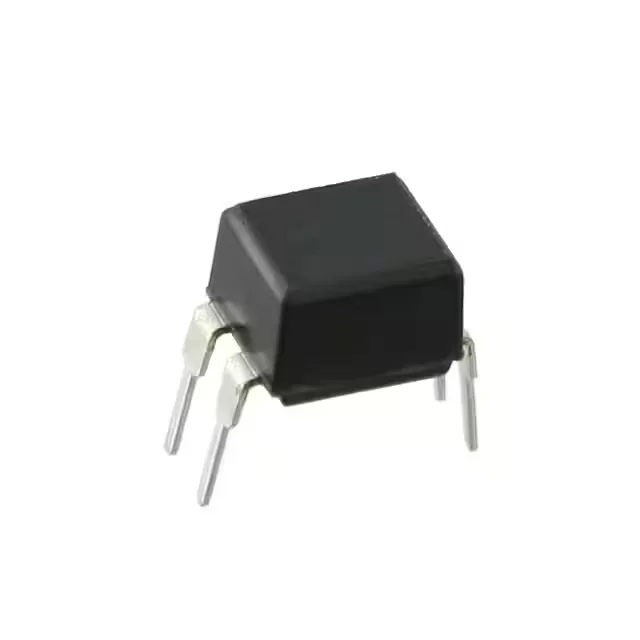
Isolation barrier and CTR — the two numbers that decide the BOM fit
The FOD817D delivers 5000 Vrms isolation between input and output — this is the peak test voltage the part withstands for one minute per UL 1577, not a working voltage. For reinforced isolation at mains voltages, the working voltage rating must be derated from the peak test figure; a 5000 Vrms test typically supports a 250 Vrms working voltage in pollution degree 2, but the actual system creepage and clearance still govern the safety approval. Current transfer ratio is specified as a range: 300% minimum to 600% maximum at If = 5 mA. This means the output transistor can sink 3 to 6 times the LED current — a 5 mA forward current yields 15 to 30 mA of output drive capability. The wide CTR spread matters for production yield: the design must work at the 300% floor, not the typical value, because the actual CTR of any single unit is unknown until tested. Vce(sat) is 200 mV maximum at the rated output current — this is the voltage dropped across the phototransistor when fully on. In a 5 V logic interface, the 200 mV saturation leaves 4.8 V at the output pin, well above the VIH threshold of most CMOS inputs. For higher-side switching near the 70 V output maximum, the saturation voltage adds to the load voltage drop and must be budgeted in the power dissipation calculation.
Temperature range and switching speed for industrial control
Operating temperature spans -55°C to +110°C, covering industrial enclosures and under-hood automotive zones without derating. The 4 µs rise and 3 µs fall times (typical) set the maximum data rate to roughly 100 kbit/s in a saturated switch application — fast enough for 50/60 Hz line synchronisation, PLC digital inputs, and DC bus voltage feedback, but not for high-speed serial isolation. Forward voltage is 1.2 V typical at If = 20 mA, and the absolute maximum forward current is 50 mA DC. The DC input type means the LED conducts only one polarity — reverse-voltage protection is needed if the drive source can swing negative.