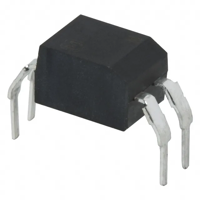
The FOD817AW is officially marked as Obsolete by onsemi, meaning the manufacturer has discontinued production and no further factory orders are accepted.
Isolation and signal transfer — what the ratings mean
The 5000Vrms isolation rating certifies galvanic separation between input and output for safety and noise immunity in industrial, medical, and power-supply applications — the 4-DIP package provides the creepage distance to sustain that voltage without breakdown. Current transfer ratio spans 80% to 160% at a forward current of 5 mA, giving the designer a guaranteed minimum CTR for logic-level interfacing — the 200mV max Vce saturation keeps the output transistor's voltage drop low enough to drive a downstream gate or PLC input without a pull-up resistor adjustment. The -55°C to 110°C operating range covers industrial and automotive ambient extremes — the 4µs rise and 3µs fall times support switching frequencies up to roughly 100 kHz before the output waveform degrades.
Housed in a 4-DIP (0.400", 10.16mm) through-hole package, the FOD817AW mounts directly into a standard 0.100-inch pitch DIP socket or solders into plated through-holes on a single- or double-sided PCB — no special footprint beyond the standard 7.62 mm row spacing. The DC input and transistor output configuration is the most common optocoupler topology: the LED on the input side switches the phototransistor on the output side, providing 5000Vrms of galvanic isolation between the two circuits.