Tri-core architecture and memory budget
The SPC5748GGK1VM is a 32-bit Tri-Core MCU from the MPC57xx Qorivva family, built around three processor cores: one e200z2 and two e200z4. It runs at 80 MHz on the z2 core and up to 120 MHz on the z4 cores, giving you asymmetric multiprocessing headroom for a real-time OS on one core and application code on the other. Program memory is 6 MB of on-chip Flash (6M x 8), backed by 768K x 8 of SRAM. That Flash footprint handles a full AUTOSAR stack plus application code without external memory in most automotive body and gateway designs.
Peripheral set and signal chain
Connectivity includes CANbus, Ethernet, I²C, LINbus, SAI, and SPI — enough to serve as a domain controller bridging multiple vehicle buses. The 80-channel 10-bit and 64-channel 12-bit SAR ADCs sample analog sensors directly, with the 12-bit resolution suitable for throttle-position or pressure-sensor inputs. On-chip peripherals cover DMA, low-voltage detect (LVD), power-on reset (POR), and watchdog timer (WDT).
Package, supply, and temperature grade
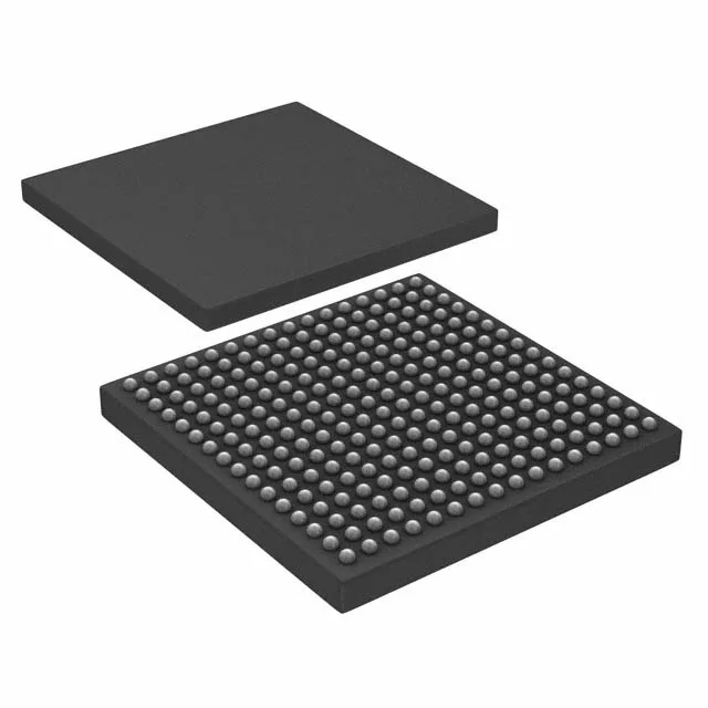
Housed in a 256-ball LBGA (17x17 mm MAPBGA), the SPC5748GGK1VM is a surface-mount BGA. The 1.08 V to 1.32 V core supply means a dedicated 1.2 V rail is needed, separate from the 3.3 V I/O supply — plan for a dual-output regulator or two discrete LDOs on the board. The 256-MAPPBGA footprint requires a controlled impedance stack-up for the high-speed interfaces; the BGA pitch is 1.0 mm typical for this package, so four-layer boards are standard.
Lifecycle and supply posture
The 256-LBGA package is moisture-sensitive — store the reels in a dry cabinet or bake before reflow if the moisture-barrier bag is compromised.