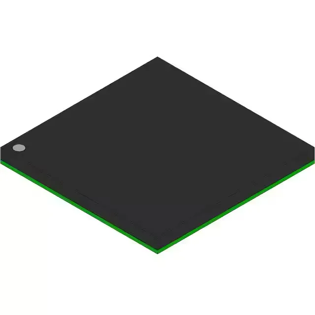
NXP Semiconductors SPC5747GBK1VMJ6 — Microcontrollers & Processors (MCU / MPU / DSP)

SPC5747GBK1VMJ6 MCU, MPC57xx, Tri-Core, 4MB Flash

MPNSPC5747GBK1VMJ6
End of Life

NXP SPC5747GBK1VMJ6, MPC57xx series, 32-bit Tri-Core MCU, 4MB FLASH, 768K x 8 RAM, 80MHz/160MHz, 256-MAPPBGA (17x17), -40°C to 105°C.

$37.62Ref. price · indicative, final on quote
Packaging256-LBGA
SeriesMPC57xx
Sourced new & surplus through independent channelsAuthenticity-screened · ESD-safe packingListing updated Aug 2026

Specifications

SPC5747GBK1VMJ6 specifications
ParameterValue
SeriesMPC57xx
MountingSurface Mount
Oscillator typeInternal
Program memory typeFLASH
Voltage - supply (Vcc (Vdd))3V ~ 5.5V
Operating temperature-40°C ~ 105°C (TA)
Speed80MHz/160MHz
PackageBulk
RAM size768K x 8
Core size32-Bit Tri-Core
PeripheralsDMA, LVD, POR, WDT
ConnectivityCANbus, Ethernet, I²C, LINbus, SAI, SPI, USB, USB OTG
Number of i (O)178
Core processore200z2, e200z4, e200z4
Case256-LBGA
Data convertersA/D 80x10b, 64x12b
Program memory size4MB (4M x 8)

Product details

Tri-core architecture and clock domains

The SPC5747GBK1VMJ6 is a 32-bit Tri-Core microcontroller from the MPC57xx series, built around one e200z2 core clocked at 80 MHz and two e200z4 cores at 160 MHz. This asymmetric multiprocessing arrangement lets the slower core handle safety-monitoring and real-time housekeeping while the faster pair run the application logic and communications stack.

Memory budget and program storage

On-chip program memory is 4 MB of flash (4M x 8), paired with 768 KB of SRAM. The flash holds the firmware image and calibration data; the RAM budget must accommodate the AUTOSAR or safety stack, communication buffers, and the application heap. With 178 I/O lines, the device can drive parallel memory buses or a wide sensor array without external GPIO expanders.

Connectivity and analog front-end

The peripheral set includes CANbus, Ethernet, USB OTG, I²C, LINbus, SAI, and SPI — covering both automotive in-vehicle networks and industrial fieldbus interfaces. The analog subsystem provides 80 channels of 10-bit ADC and 64 channels of 12-bit ADC, enough to read multiple sensor inputs without external multiplexing.

Frequently asked questions

What is the core architecture and clock speed of SPC5747GBK1VMJ6?

The device uses a 32-bit Tri-Core architecture with one e200z2 core running at 80 MHz and two e200z4 cores at 160 MHz, providing separate domains for safety monitoring and application processing.

What is the memory configuration of SPC5747GBK1VMJ6?

It has 4 MB of on-chip flash program memory and 768 KB of SRAM, sufficient for complex control firmware with safety stacks and communication buffers.