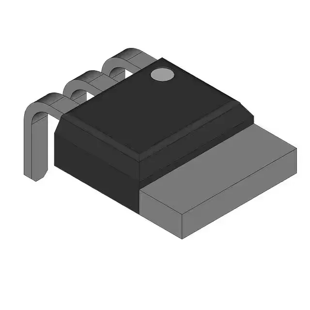
A 100 V, 97 A N-channel MOSFET in a through-hole I2PAK
It comes in a TO-262-3 (I2PAK) through-hole package, which handles the 183 W power dissipation without relying solely on PCB copper — the tab carries the heat to a heatsink or chassis.
The 44.5 nC typical gate charge at 10 V is moderate for a 97 A device — a standard gate driver with 1 A peak output will switch it in the tens of nanoseconds. The input capacitance of 3181 pF at 50 V drain-source means the driver sees a capacitive load that rises with lower Vds; budget for that in the gate-drive loop inductance. The drive voltage range (7 V to 10 V for rated Rds(on)) lets you use a 12 V rail with a 10 V gate clamp, or a 10 V rail directly. The ±20 V Vgs(max) gives headroom for ringing on long gate traces, but a 15 V zener clamp is still cheap insurance.
Where it fits — motor control and power conversion
With 100 V blocking and 97 A continuous rating, this MOSFET is a natural fit for 48 V to 72 V DC bus motor drives (brushless DC, PMSM), battery-management disconnect switches, and DC-DC converters in the 500 W to 1 kW range. The through-hole I2PAK package is easier to heatsink than a surface-mount D2PAK for the same dissipation — a single M3 screw and a TO-220-style clip mount the tab to a chassis or extruded heatsink. The 175°C junction maximum means the part can survive short-duration overloads in a 105°C ambient if the thermal path is sized correctly.
Lifecycle — active, no LTB signal
Nexperia lists the PSMN8R5-100ESFQ as Active. The active status also means Nexperia continues to support it with datasheet revisions and application notes.