267 MHz PowerPC e300c3 — where the clock lands vs the rest of the MPC83xx family
The MPC8313CZQADDC runs a single PowerPC e300c3 core at 267 MHz — 32-bit wide, clocked below the 400 MHz MPC8360CZUAGDGA but in the same range as the 266 MHz MPC8343CZQADDB and the 266 MHz MPC8323EZQADDC. For control-plane packet processing or I/O aggregation, the 267 MHz ceiling is the throughput governor; the memory controller and Ethernet MACs will idle before the core saturates in most bridging or protocol-conversion applications.
USB 2.0 + PHY — one integrated port vs the two-PHY peer
This part integrates a single USB 2.0 port with its own PHY on-die — one external PHY chip eliminated from the BOM compared to the MPC8343CZQADDB, which carries USB 2.0 + PHY (2). For designs needing only one USB host/device port, the MPC8313 saves the component count and board area; a two-port requirement pushes the BOM toward the MPC8343 or an external hub controller.
Dual Gigabit Ethernet — same MAC count as the 8343, but the core clock determines wire-rate margin
Two 10/100/1000 Mbps Ethernet ports are on-die — the same MAC count as the MPC8343CZQADDB (which carries three). At 267 MHz, the core has enough headroom to forward two 1 Gbps streams without dropping packets in a simple bridge configuration, but adding encryption or deep-packet inspection will eat into the margin. The MPC8360CZUAGDGA at 400 MHz with a QUICC Engine co-processor is the better fit for line-rate security processing.
Industrial temp range — -40 to 105 °C, full automotive/industrial grade
Rated for -40 to 105 °C ambient — this is the full industrial temperature grade, not the commercial 0 to 70 °C cut. The 516-TEPBGA exposed-pad package relies on a good thermal via array under the pad to keep the junction below the 105 °C limit at full load; board designers should budget a 2x2 or 3x3 grid of thermal vias connected to an internal ground plane.
Memory controller — DDR and DDR2 support, no DDR3
The integrated memory controller supports both DDR and DDR2 SDRAM — not DDR3. This gives the board designer flexibility to use either memory generation depending on cost and availability, but caps peak memory bandwidth below what a DDR3 controller delivers. Typical configurations pair this processor with DDR2-533 or DDR-400 in a 32-bit or 64-bit bus width.
Peripheral set — DUART, HSSI, I²C, PCI, SPI
The additional interfaces cover the common control-plane and data-plane connections: DUART for console/debug serial, HSSI for high-speed serial links, I²C and SPI for sensor/management bus peripherals, and PCI for legacy parallel-bus add-on cards. No SATA or PCIe — designs requiring those buses need an external bridge or a different processor family.
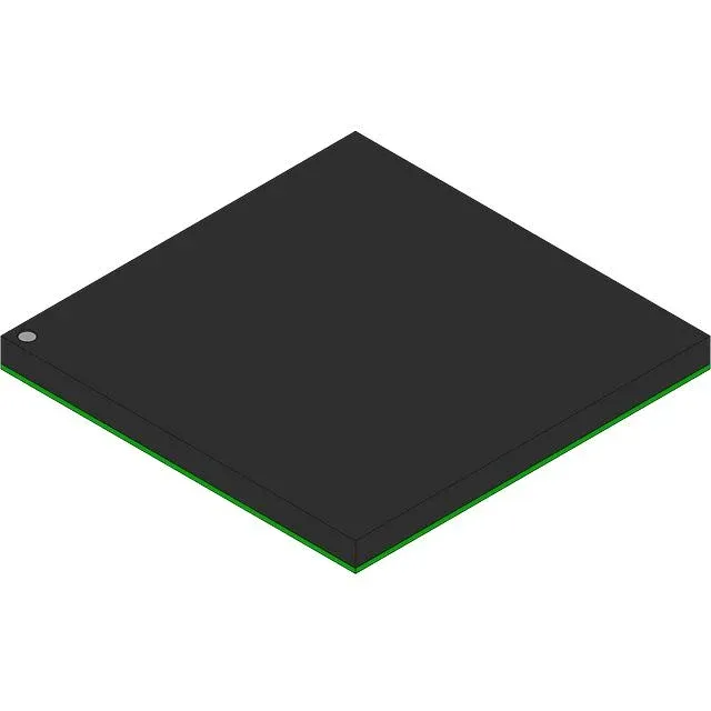
Package and board integration — 516-TEPBGA (27x27 mm)
The 516-ball BGA with exposed thermal pad measures 27x27 mm body. The exposed pad requires a solder paste stencil opening that covers at least 50% of the pad area for reliable thermal and electrical contact. Standard reflow profile for SnPb BGA: ramp to 183 °C at 1-2 °C/s, soak 60-90 s above 183 °C, peak 215-225 °C.