133 MHz PowerPC e300c3 with on-chip QUICC Engine
The MPC8306SCVMABDCA is a single-core PowerQUICC II Pro system-on-chip built around the PowerPC e300c3 core running at 133 MHz. It integrates a QUICC Engine co-processor that handles communications protocol processing independently from the main core, freeing CPU cycles for application code. On-chip connectivity includes one USB 2.0 port and three 10/100 Mbps Ethernet MACs, making this SoC suited for industrial gateways, protocol converters, and networked control applications where multiple wired interfaces terminate at a single processor.
Industrial temperature grade and memory interface
The integrated DDR2 memory controller supports standard DDR2 SDRAM, which at 133 MHz core speed provides adequate memory bandwidth for packet buffering and control-plane data. The 32-bit data bus width keeps the PCB routing density manageable on a 4-layer board.
Peripheral set and package footprint
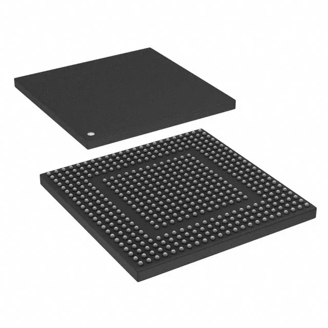
Additional serial interfaces include DUART, I²C, SPI, and TDM — covering the common control buses for industrial sensors, motor drives, and fieldbus PHYs. The TDM port can connect to an external T1/ framer or a multi-channel codec for voice or telemetry streams. Housed in a 369-ball PBGA package measuring 19x19 mm (supplier device package 369-PBGA), the ball pitch is 0.80 mm — routable on a 4-layer PCB with standard via technology. The surface-mount package requires a solder reflow profile per JEDEC J-STD-020 for the lead-free solder balls.
Active lifecycle — sourcing posture
The part ships in bulk packaging as standard.