Active production — what it means for a BOM line
The MPC536CZP40: RoHS non-compliant — the 388-PBGA package uses leaded solder balls. If your assembly line is RoHS-exempt (medical, military, or high-rel per EU exemption 7c-I), this is a non-issue; otherwise budget for a leaded process or a Pb-free alternative.
40 MHz PowerPC — memory and peripheral fit
A 32-bit single-core PowerPC clocked at 40 MHz with 1 MB of on-chip Flash and 36K x 8 of RAM. The Flash is large enough for a full RTOS image plus application code in automotive or industrial control; the 36K RAM is the working-memory ceiling — a heavy CAN stack with multiple message buffers will eat into that quickly, so budget the SRAM before committing the BOM. The POR, PWM, and WDT peripherals cover brown-out reset, variable-duty-cycle outputs, and watchdog supervision without external glue. Connectivity includes CANbus, EBI/EMI, SCI, SPI, and UART/USART — the CAN controller makes this MCU a natural fit for automotive body electronics or industrial fieldbus gateways. The external oscillator lets you choose a crystal or MEMS clock source; the aperture-jitter budget is yours to set.
Industrial temperature and BGA footprint
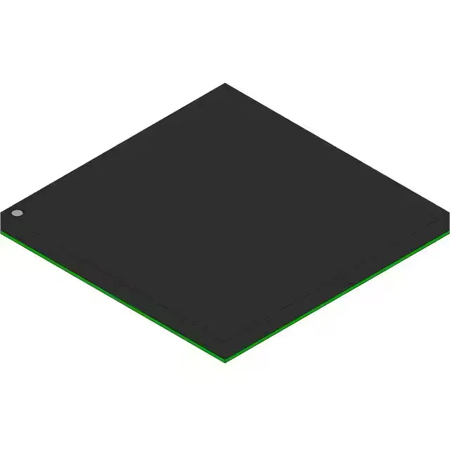
The 388-PBGA (27x27 mm body,) demands a controlled reflow profile; a 4-layer or 6-layer PCB is typical for fan-out of the 388 balls. Supply voltage is 2.5 V to 2.7 V — a narrow window that requires a regulated rail. A 2.5 V LDO with ±2% tolerance keeps the core inside the band; a 3.3 V I/O section is not present on this die, so all external interfaces must level-shift if the peripheral rail is higher. Surface-mount BGA — the 1.27 mm ball pitch is forgiving for a standard SMT line, but the 27 mm body means the board must survive the CTE mismatch during reflow. A moisture-sensitive-device bake before assembly is recommended if the storage log shows exposure above the floor life.