NXP Semiconductors MMPF0100F9ANESR2 — Microcontrollers & Processors (MCU / MPU / DSP)

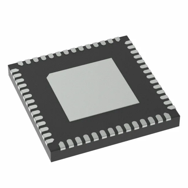
MMPF0100F9ANESR2 NXP i.MX6 PMIC, 12 outputs, 56-QFN

MPNMMPF0100F9ANESR2
End of Life

NXP Semiconductors MMPF0100F9ANESR2 power management IC, 12-output converter for i.MX6, 2.8V-4.5V input, 56-VFQFN Exposed Pad, surface mount wettable flank, -40°C to +105°C.

$10.04Ref. price · indicative, final on quote
Packaging56-VFQFN Exposed Pad
RoHSROHS3 Compliant
Independent supplier — new & surplus stockAuthenticity-screened · ESD-safe packingListing updated Aug 2026

Specifications

MMPF0100F9ANESR2 specifications
ParameterValue
MountingSurface Mount, Wettable Flank
Voltage - input2.8V ~ 4.5V
Voltage - outputMultiple
I/O channels12
Operating temperature-40°C ~ 105°C (TA)
PackageTape & Reel (TR); Cut Tape (CT)
ApplicationsConverter, i.MX6
Case56-VFQFN Exposed Pad

Product details

PMIC for i.MX6 — twelve rails in one 56-QFN package

The NXP MMPF0100F9ANESR2 is a power management IC that integrates twelve regulated outputs specifically sequenced for the i.MX6 processor family. It accepts a 2.8 V to 4.5 V input — typically a single Li-ion cell or 3.3 V intermediate rail — and generates the multiple core, memory, and I/O voltages the i.MX6 needs without external sequencing logic. The 56-VFQFN Exposed Pad package (8x8 mm) with wettable flank terminals supports automated optical inspection (AOI) of solder joints, a requirement for high-reliability assembly.

Rail budget and thermal envelope

Twelve outputs cover the full i.MX6 power tree: the core supply (VDDARM, VDDSOC), DDR memory rail, I/O banks, PLLs, and USB PHY — each programmable via I2C for voltage and sequencing.

Frequently asked questions

What is the MMPF0100F9ANESR2 used for?

It is a power management IC (PMIC) designed for NXP i.MX6 application processors, providing twelve programmable voltage rails and sequencing in a single 56-QFN package.