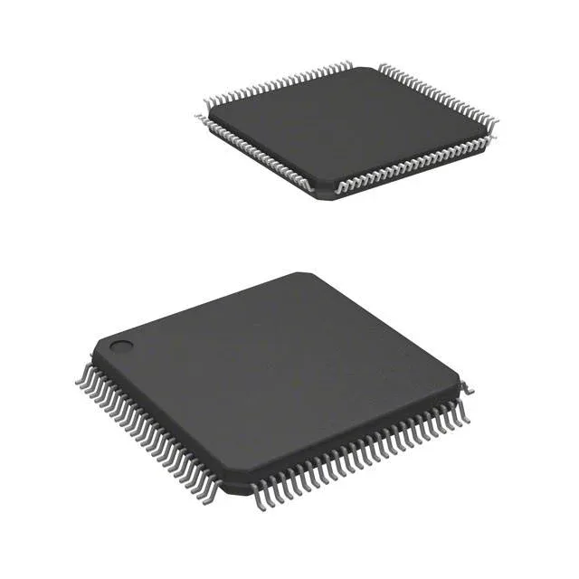
100 MHz Cortex-M4 with on-chip signal-chain peripherals
The MK51DX256CLL10: The Cortex-M4 core includes a single-cycle multiply-accumulate unit and a hardware floating-point engine, so the part handles real-time control loops and sensor fusion without an external DSP. On-chip memory partitions 256 KB of program flash, 64 KB of SRAM, and 4 KB of EEPROM. The flash and RAM are sufficient for a mid-complexity application stack — a motor-control FOC library plus a USB communication stack fits within the 256 KB budget, leaving headroom for field-upgradeable firmware. The analog front end integrates a 35-channel, 16-bit ADC and two 12-bit DACs. The 16-bit ADC resolution is enough for precision current sensing in servo drives or for multi-channel data acquisition without an external ADC.
Supply, temperature, and package for board integration
The wide range allows direct connection to a 3.3 V sensor bus without a separate regulator for the core. Suitable for factory-floor controllers, outdoor telecom equipment, and automotive cabin applications that do not require AEC-Q100 qualification. Housed in a 100-LQFP package with a 14x14 mm body and 0.5 mm pitch. Standard reflow profile for LQFP-100 applies.
Connectivity and peripheral set for system-level design
The connectivity block includes USB OTG (host/device), I²C, SPI, UART/USART, and IrDA. USB OTG enables the MCU to act as a USB host for a flash drive or as a device for firmware updates over a virtual COM port. Additional peripherals: DMA controller for memory-to-peripheral transfers without CPU intervention, an LCD controller for segment displays, a PWM timer for motor or LED dimming, a low-voltage detect (LVD) for brown-out protection, and a watchdog timer. 59 general-purpose I/O pins are available in the 100-LQFP package. The I/O count supports a 16x2 character LCD, a 4x4 keypad, and several serial interfaces simultaneously.
Lifecycle and compliance status
RoHS3 compliant (2011/65/EU + 2015/863) — no exemption-based restrictions. The part is supplied in a tray, suitable for pick-and-place assembly without additional moisture-sensitive handling beyond the standard LQFP bake-out procedure.