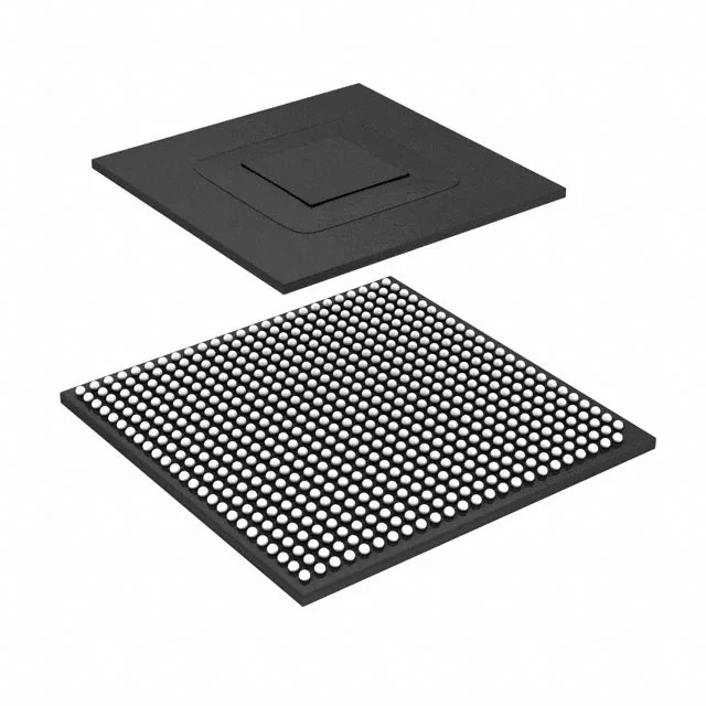
NXP Semiconductors MCIMX6U7CVM08AC — Memory (DRAM / SRAM / Flash / EEPROM)

NXP i.MX6DL MCIMX6U7CVM08AC ARM Cortex-A9 MPU, 800MHz

MPNMCIMX6U7CVM08AC
End of Life

NXP i.MX6DL series, ARM Cortex-A9 MPU, MCIMX6U7CVM08AC, 2 Core 32-Bit, 800MHz, LPDDR2/LVDDR3/DDR3, USB 2.0 + PHY (4), Ethernet 10/100/1000Mbps (1), -40°C ~ 105°C, 624-MAPBGA (21x21).

$57.12Ref. price · indicative, final on quote
Packaging624-LFBGA
StockContact for availability
MOQ1 pcs
  • 100% new & originalTraceable channels only — no refurbs, no pulls, no remarked parts.
  • Date & lot codes on quoteStated per line before you commit; label photos on request.
  • MSL-compliant ESD packingMoisture-sealed bags with indicator cards; reels photo-verified.
  • PayPal buyer protectionPay by T/T, PayPal or Payoneer — card payments covered end to end.

Specifications

MCIMX6U7CVM08AC Technical Specifications
ParameterValue
Seriesi.MX6DL
Mounting typeSurface Mount
Voltage - i (O)1.8V, 2.5V, 2.8V, 3.3V
Additional interfacesCAN, I²C, I²S, MMC/SD/SDIO, SAI, SPI, SSI, UART
Display & interface controllersKeypad, LCD
Operating temperature-40°C ~ 105°C (TA)
Number of cores (Bus width)2 Core, 32-Bit
USBUSB 2.0 + PHY (4)
Speed800MHz
PackageTray
Ethernet10/100/1000Mbps (1)
Core processorARM® Cortex®-A9
Case624-LFBGA
RAM controllersLPDDR2, LVDDR3, DDR3
Co-Processors (DSP)Multimedia; NEON™ SIMD
Security featuresARM TZ, Boot Security, Cryptography, RTIC, Secure Fusebox, Secure JTAG, Secure Memory, Secure RTC, Tamper Detection
Graphics accelerationYes

Product details

Dual-core Cortex-A9 at 800 MHz — what it means for the BOM

The MCIMX6U7CVM08AC is a dual-core ARM Cortex-A9 application processor clocked at 800 MHz per core. The 624-MAPBGA package (21x21 mm) routes memory and peripheral signals on a single board layer if the layout is tight.

Industrial temperature range — -40°C to 105°C

Rated for -40°C to 105°C ambient, this part handles outdoor telecom cabinets, motor-drive enclosures, and engine-bay-adjacent controllers without a heater or active cooling fan.

Peripherals — USB 2.0 + PHY, Gigabit Ethernet

Four USB 2.0 ports with integrated PHY eliminate external transceiver chips — saves board area and BOM cost. A single Gigabit Ethernet MAC (10/100/1000 Mbps) is enough for one network interface; if you need dual redundant ports for ring topologies, plan on an external switch or a second MAC via the PCIe lane. Additional interfaces include CAN, I²C, I²S, SPI, UART, and SDIO — covers most sensor and actuator buses on an industrial control board.

Graphics and security hardware

Hardware graphics acceleration and LCD/keypad controllers are built in — useful for local HMI displays without a separate GPU chip. The security block includes ARM TrustZone, secure boot, cryptography, tamper detection, and secure RTC.

Lifecycle and sourcing — still in active production

The MCIMX6U7CVM08AC is an active, current-production part (ROHS3 compliant). No last-time-buy risk on the horizon. NXP continues to manufacture the series alongside the newer i.MX8 series, so supply is stable through authorized and independent channels. We source and quote to order against an RFQ.

Frequently asked questions

What is the difference between MCIMX6U7CVM08AC and MCIMX6U7CVM08AB?

The 'AC' and 'AB' suffixes denote different silicon revisions or stepping levels. The MCIMX6U7CVM08AC is the newer revision, incorporating any errata fixes and process improvements from the AB stepping. For new designs, use the AC revision.

What is the operating temperature of MCIMX6U7CVM08AC?

The operating temperature range is -40°C to 105°C (ambient), suitable for industrial and outdoor applications.

What USB interfaces does MCIMX6U7CVM08AC have?

It includes four USB 2.0 ports with integrated PHY, eliminating the need for external transceivers.

What is the core speed of MCIMX6U7CVM08AC?

The dual-core ARM Cortex-A9 runs at 800 MHz per core.