Dual Cortex-A9 at 1 GHz — processing headroom for industrial control
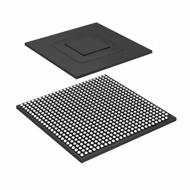
The MCIMX6U6AVM10AC is a dual-core ARM Cortex-A9 processor from NXP's i.MX6DL series, clocked at 1 GHz. Two 32-bit cores with NEON SIMD multimedia coprocessing give it the throughput for an HMI panel running a real-time OS alongside a graphics stack, or for a multi-axis motion controller that decodes EtherCAT frames and updates the servo loop in the same cycle. The 1 GHz speed rating is the maximum operating frequency across the full -40 to 125 °C junction temperature range — no derating required when the enclosure sits in a non-conditioned factory bay or inside an engine-bay ECU. That temperature grade is the industrial and automotive junction band; the part sustains full clock rate at 105 °C ambient with the right thermal management on the 21x21 mm MAPBGA package.
Integrated peripherals — what the board-level designer needs to know
Four USB 2.0 ports with integrated PHY and one Gigabit Ethernet MAC (10/100/1000 Mbps) mean the processor can serve as the central node in a machine network without external PHY chips for the USB side — the Ethernet still needs an external PHY, but the MAC is on-die. The memory interface supports LPDDR2, LVDDR3, and DDR3, giving the layout engineer flexibility to choose the memory density and voltage plane that matches the system power budget. The additional interface list covers CAN, I²C, I²S, SPI, UART, and MMC/SD/SDIO, which is the full set for an industrial gateway or a data-acquisition front end. Security features include ARM TrustZone, secure boot, cryptography acceleration, a secure real-time clock, and tamper detection. For a system that logs production data or stores calibration constants, the secure RTC and tamper detection prevent clock rollback and enclosure-opening attacks without a separate security co-processor.
Package and temperature — the layout engineer's constraints
The 624-MAPBGA (21x21 mm) package is a 0.80 mm ball pitch — a four-layer PCB with via-in-pad or microvias is the practical minimum for fan-out. The supplier device package is the same 624-MAPBGA (21x21 mm), so the footprint is consistent across the i.MX6DL family. Operating temperature range is -40 to 125 °C junction — the board's FR4 Tg and the solder joint's thermal cycle life become the limiting factors, not the silicon. For a rework lab tech, the MAPBGA package needs a pre-bake at 125 °C for 8 hours if the moisture-sensitive level (MSL) floor is exceeded; the part's ROHS3 compliance means lead-free solder profile with a peak reflow around 245-260 °C.
Active lifecycle and compliance — no end-of-life pressure
ROHS3 compliant — no exemption expiry to track for the bill of materials. The part is supplied in tray packaging, which is the standard for MAPBGA devices in production volumes; the tray quantity is confirmed at RFQ.