Dual-core Cortex-A9 at 1.0 GHz
The MCIMX6U5DVM10ACR is a dual-core ARM Cortex-A9 processor from the i.MX6DL series, clocked at 1.0 GHz. Each core is a 32-bit unit, giving the part a symmetric multiprocessing capability for running a main OS and a real-time task on separate cores without a hypervisor.
Memory and peripheral integration
Memory controllers support LPDDR2, LVDDR3, and DDR3, giving the BOM flexibility to use whichever DRAM type is most cost-effective at the target density. On the peripheral side, four USB 2.0 ports with integrated PHY eliminate external transceivers for most designs, and the single Gigabit Ethernet MAC (10/100/1000 Mbps) connects directly to an external PHY via the RGMII interface. Additional interfaces include CAN, I²C, I²S, MMC/SD/SDIO, SAI, SPI, SSI, and UART, covering the common control and audio buses for an embedded system. The display controller handles keypad and LCD outputs, while the dedicated graphics acceleration block offloads 2D/3D rendering from the CPU cores.
Package, temperature, and rework considerations
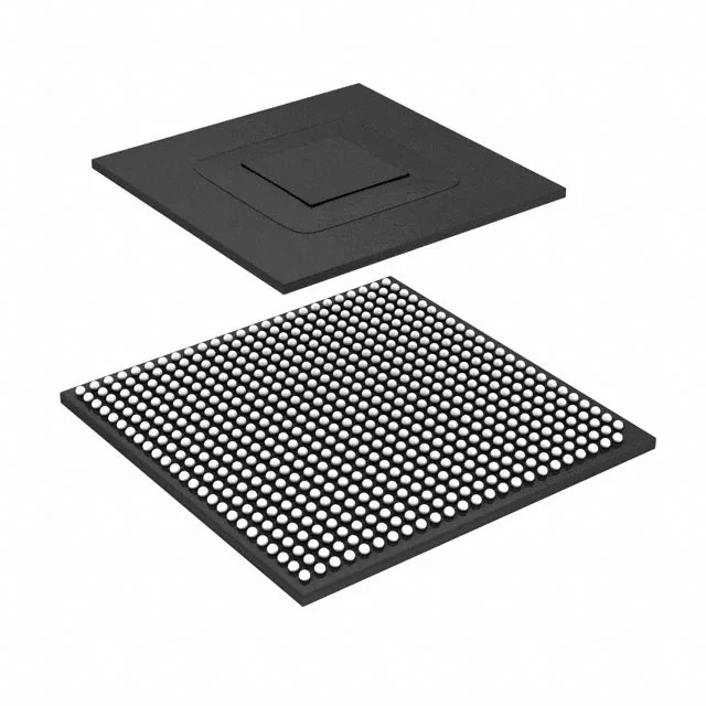
Housed in a 624-ball MAPBGA (21x21 mm), the part is surface-mount only. The 0.8 mm ball pitch is reworkable with a good hot-air station and a stencil, but the large array means the board must be dry before reflow — the 0°C to 95°C junction temperature range is the operating envelope, not a storage spec, so the moisture sensitivity level (MSL) on the reel label governs bake requirements before rework. The 1.8V, 2.5V, 2.8V, and 3.3V I/O voltage rails mean the core runs on a separate supply from the memory and peripheral banks — a multi-rail PMIC or discrete LDOs are needed, not a single rail.
Security and compliance
On-chip security features include ARM TrustZone, boot security, cryptography, a secure fuse box, secure JTAG, secure memory, a secure RTC, and tamper detection. This qualifies the part for payment terminals, secure gateways, and any application where the boot chain must be locked against modification.