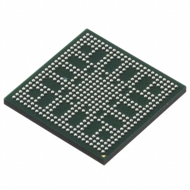
NXP Semiconductors MCIMX6L3EVN10AB — Microcontrollers & Processors (MCU / MPU / DSP)

NXP MCIMX6L3EVN10AB i.MX6SL Cortex-A9 1.0GHz MPU

MPNMCIMX6L3EVN10AB
End of Life

NXP Semiconductors i.MX6SL series, ARM Cortex-A9 microprocessor, MCIMX6L3EVN10AB, 1.0GHz core, 432-MAPBGA 13x13 mm, -40 to 105°C, ROHS3.

$32.27Ref. price · indicative, final on quote
Packaging432-TFBGA
StockIn Stock (19)
Lead timeIn Stock wk
MOQ1 pcs
  • 100% new & originalTraceable channels only — no refurbs, no pulls, no remarked parts.
  • Date & lot codes on quoteStated per line before you commit; label photos on request.
  • MSL-compliant ESD packingMoisture-sealed bags with indicator cards; reels photo-verified.
  • PayPal buyer protectionPay by T/T, PayPal or Payoneer — card payments covered end to end.

Specifications

MCIMX6L3EVN10AB Technical Specifications
ParameterValue
Seriesi.MX6SL
Mounting typeSurface Mount
Voltage - i (O)1.2V, 1.8V, 3.0V
Additional interfacesAC97, I2C, I2S, MMC/SD/SDIO, SPI, SSI, UART
Display & interface controllersKeypad, LCD
Operating temperature-40°C ~ 105°C (TA)
Number of cores (Bus width)1 Core, 32-Bit
USBUSB 2.0 + PHY (3)
Speed1.0GHz
PackageTray
Ethernet10/100Mbps (1)
Core processorARM® Cortex®-A9
Case432-TFBGA
RAM controllersLPDDR2, LVDDR3, DDR3
Co-Processors (DSP)Multimedia; NEON™ SIMD
Security featuresARM TZ, Boot Security, Cryptography, RTIC, Secure Fusebox, Secure JTAG, Secure Memory, Secure RTC, Tamper Detection
Graphics accelerationYes

Product details

Core architecture and clock budget for the BOM line

The MCIMX6L3EVN10AB is a single-core ARM Cortex-A9 application processor from the NXP i.MX6SL series, running at 1.0 GHz. This is the maximum core frequency; actual throughput depends on the flash wait-state profile and the memory controller configuration. The NEON SIMD coprocessor handles single-instruction multiple-data (SIMD) operations for multimedia and signal-processing tasks without loading the Cortex-A9 pipeline. Graphics acceleration is present on-die, driving the LCD display controller. Memory controller supports LPDDR2, LVDDR3, and DDR3 — the board designer picks the memory type that matches the target cost and speed grade. The 432-MAPBGA (13x13 mm) package requires a 4-layer PCB minimum for fan-out of the 0.50 mm pitch balls.

Peripheral set and connectivity for system integration

The single 10/100 Ethernet MAC with on-chip PHY provides wired networking without an external magnetics module — the PHY is internal, so only the RJ45 connector and isolation transformer are needed on the board. Additional interfaces include AC97, I2C, I2S, MMC/SD/SDIO, SPI, SSI, and UART — covering audio codec, touch controller, storage, and serial debug. The I/O voltage rails are 1.2 V, 1.8 V, and 3.0 V, requiring three separate supply domains on the PCB. Security features are hardware-enforced: ARM TrustZone, boot security, cryptography engine, secure fuse box, secure JTAG, secure memory, secure RTC, and tamper detection. These blocks run independently of the Cortex-A9 core, so secure boot and key storage do not consume application MIPS.

An outdoor IoT gateway or factory controller that sees 85°C on a summer production floor still has 20°C of margin before the silicon junction hits the rated limit. Production status is active per NXP's lifecycle record. The part is ROHS3 compliant, meeting the EU RoHS exemption 7(c)-I for lead in solder.

Frequently asked questions

What memory types does the MCIMX6L3EVN10AB memory controller support?

The on-chip memory controller supports LPDDR2, LVDDR3, and DDR3. The board designer selects the memory type based on cost, speed, and voltage requirements — all three are single-rail interfaces that connect directly to the processor without an external memory controller.

What is the USB configuration on the MCIMX6L3EVN10AB?

The processor integrates three USB 2.0 ports, each with its own on-chip PHY. This means no external USB transceiver is required — the differential D+/D- lines route directly from the package balls to the USB connector.