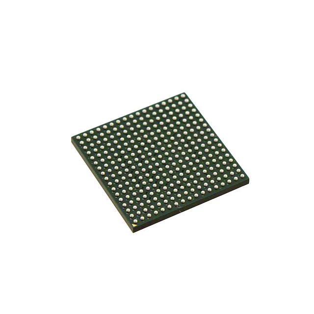
ARM926EJ-S at 454 MHz — processing headroom for HMI and IoT gateways
The MCIMX283DVM4BR2 is an NXP i.MX28 series application processor built around a single ARM926EJ-S core clocked at 454 MHz. This puts it in the class of mid-range embedded MPUs suitable for human-machine interfaces, industrial IoT gateways, and networked control panels where the processing load includes a graphical display, Ethernet communication, and multiple serial peripherals. The 454 MHz ceiling is the maximum operating frequency; actual throughput depends on the flash wait-state profile and the memory bus speed, but the core itself can sustain the DMIPS level typical of an ARM926EJ at this clock.
Memory interface — LVDDR, LVDDR2, DDR2 flexibility
The integrated memory controller supports LVDDR, LVDDR2, and DDR2 SDRAM, giving the board designer a choice of memory technology based on cost, availability, and speed requirements. LVDDR2 runs at lower voltage than standard DDR2, which can simplify the power rail design in a mixed-voltage system. The 289-ball LFBGA package (14x14 mm MAPBGA) routes the memory interface signals on a 0.80 mm pitch — a four-layer PCB is typical for fan-out, though a well-planned six-layer board improves signal integrity on the DDR2 clock and strobe lines.
Connectivity — dual USB 2.0 with PHY, single Ethernet MAC
Two USB 2.0 ports each integrate the PHY on-chip, eliminating the need for external USB transceivers and reducing BOM cost. The ports can operate as host, device, or OTG, which is useful for a gateway that connects to a USB cellular modem and a USB flash drive simultaneously. A single 10/100 Mbps Ethernet MAC with integrated PHY provides the wired network interface. The MAC supports IEEE 1588 precision time protocol, which matters for synchronised data acquisition or motion control applications over Ethernet.
Peripheral set and security — I2C, SPI, UART, SDIO plus hardware cryptography
The additional interfaces include I2C, I2S, MMC/SD/SDIO, SAI, SPI, SSI, SSP, and UART — enough to connect a touchscreen controller, audio codec, SD card storage, and multiple sensors without external GPIO expanders or muxes. Security features cover boot security, hardware cryptography, and a hardware unique ID. The DCP (Data Co-Processor) offloads cryptographic operations (AES, SHA, RSA) from the ARM core, so secure boot and encrypted communication do not steal cycles from the application. The display and interface controllers support keyboard, LCD, and touchscreen — a single MCIMX283DVM4BR2 can drive a QVGA or WQVGA panel and read a resistive touch overlay directly.
Active lifecycle and compliance posture
ROHS3 compliant means the part meets the latest EU RoHS exemption limits, including for the four phthalates added in Directive 2015/863. No special handling or documentation waivers are needed for EU-market equipment.