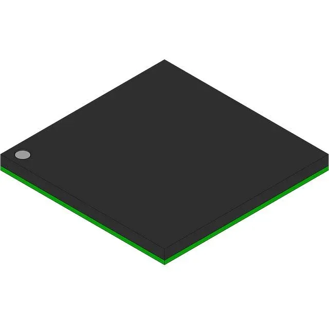
NXP Semiconductors MCF54410CMF250 — Microcontrollers & Processors (MCU / MPU / DSP)

MCF54410CMF250 ColdFire V4 MCU, 250 MHz, 196-BGA

MPNMCF54410CMF250
End of Life

NXP MCF5441x ColdFire V4 32-bit MCU, MCF54410CMF250, 250 MHz, 64K x 8 RAM, 196-BGA, Ethernet, USB OTG, -40 to 85°C.

$10.35Ref. price · indicative, final on quote
Packaging196-BGA
RoHSROHS3 Compliant
SeriesMCF5441x
Sourced new & surplus through independent channelsAuthenticity-screened · ESD-safe packingListing updated Aug 2026

Specifications

MCF54410CMF250 specifications
ParameterValue
SeriesMCF5441x
MountingSurface Mount
Oscillator typeInternal
Program memory typeROMless
Voltage - supply (Vcc (Vdd))1.14V ~ 1.32V
Operating temperature-40°C ~ 85°C (TA)
Speed250MHz
PackageBulk
RAM size64K x 8
Core size32-Bit Single-Core
PeripheralsDMA, PWM, WDT
Connectivity1-Wire®, CANbus, EBI/EMI, Ethernet, I²C, SmartCard, SPI, SSI, UART/USART, USB, USB OTG
Number of i (O)48
Core processorColdfire V4
Case196-BGA

Product details

ColdFire V4 at 250 MHz — core performance and on-chip resources

The MCF54410CMF250 is a 32-bit single-core ColdFire V4 microcontroller running at 250 MHz. That clock rate sets the instruction throughput ceiling in real-time control loops — the CMF250 suffix confirms the speed grade, so a BOM calling for the 250 MHz variant picks this exact part, not a lower-bin sibling. On-chip SRAM is 64K x 8 (64 KB), which is the scratchpad for time-critical data — interrupt vectors, stack, and small buffers live here without DRAM latency. The core voltage rail is tight at 1.14 V to 1.32 V, so the board's 1.2 V regulator needs to hold regulation within this window under load steps from the core. The 196-MAPBGA (15x15 mm) package demands a controlled reflow profile and X-ray inspection for hidden solder joints under the BGA body.

Peripheral set — connectivity for a networked control node

The MCF54410CMF250 integrates Ethernet MAC, USB OTG, CANbus, I²C, SPI, SSI, UART/USART, and a SmartCard interface. This makes it a single-chip host for an industrial gateway or a motor-drive controller that needs both a fieldbus port and a local debug UART. With 48 general-purpose I/O lines and internal DMA, PWM, and watchdog timer peripherals, the part can handle sensor polling, pulse generation, and supervisory monitoring without external CPLD or glue logic in many designs. The internal oscillator option reduces external component count — a clean 1.2 V rail and decoupling on the BGA supply balls are the main layout constraints.

Frequently asked questions

What is the core architecture and speed of the MCF54410CMF250?

It is a 32-bit ColdFire V4 single-core processor clocked at 250 MHz. The V4 core includes a hardware multiply-accumulate unit and branch cache for deterministic loop execution.

What package does the MCF54410CMF250 use and what are the board-level implications?

The part ships in a 196-ball MAPBGA (15x15 mm, 0.80 mm pitch). The BGA footprint requires a multi-layer PCB with via-in-pad or microvia fan-out for the inner balls, and a controlled reflow profile per the JEDEC MSL rating on the reel label.

What compliance documentation is available for the MCF54410CMF250?

NXP provides RoHS3 compliance certification (2011/65/EU + 2015/863) and REACH SVHC declarations. The part is also covered by NXP's standard PCN notification process for any manufacturing changes.