Core architecture and processing headroom
The MCF5207CVM166 is a 32-bit single-core microcontroller built around the ColdFire V2 core, clocked at 166.67 MHz. This puts it in the mid-range of the MCF520x family — enough throughput for real-time control loops in motor drives, industrial I/O modules, or protocol bridging without overspending on a superscalar part. Because it is ROMless, all program code must execute from external memory via the EBI/EMI interface. The 16K x 8 on-chip SRAM serves as scratchpad or cache, not as code store — map the memory interfaces first, because the boot media choice (parallel NOR flash, NAND, or serial) determines the pin allocation and the board's BOM cost.
Package, temperature grade, and supply rails
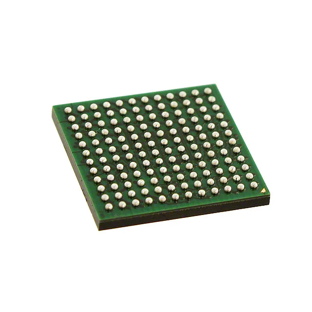
Housed in a 144-MAPBGA (13x13 mm), the package has a 0.80 mm ball pitch typical for this density. The wide tolerance also helps during power sequencing — the MCU stays in reset until the rail stabilises, so no external supervisor is strictly required for a single-rail design.
Peripheral set and system integration
On-chip peripherals include a DMA controller and a watchdog timer, plus connectivity for EBI/EMI, I²C, SPI, and UART/USART. The 30 general-purpose I/O lines are multiplexed with these interfaces — a design review of the pin mux table is needed before layout to avoid conflicts between, say, the external bus and the SPI port. The external oscillator input accepts a crystal or an active clock source. For a 166 MHz core clock, the PLL multiplies a lower-frequency reference (typically 8-16 MHz), so the board can use a commodity crystal rather than a high-frequency oscillator.
Lifecycle and compliance posture
NXP lists the MCF5207CVM166 as Active and ROHS3 compliant.